Gate-all-around (GAA) transistors offer superior electrostatic control by surrounding the channel entirely, reducing leakage and improving performance compared to multi-gate designs, which utilize multiple gates but do not fully enclose the channel. Understanding these differences can help you make informed decisions about advanced semiconductor technologies; continue reading to explore their advantages and applications in detail.
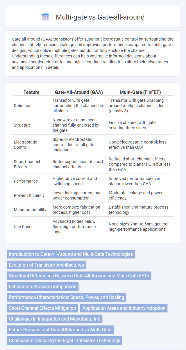
Table of Comparison
| Feature | Gate-All-Around (GAA) | Multi-Gate (FinFET) |
|---|---|---|
| Definition | Transistor with gate surrounding the channel on all sides | Transistor with gate wrapping around multiple channel sides (usually 3) |
| Structure | Nanowire or nanosheet channel fully enclosed by the gate | Fin-like channel with gate covering three sides |
| Electrostatic Control | Superior electrostatic control due to full gate enclosure | Good electrostatic control; less effective than GAA |
| Short Channel Effects | Better suppression of short channel effects | Reduced short channel effects compared to planar FETs but less than GAA |
| Performance | Higher drive current and switching speed | Improved performance over planar; lower than GAA |
| Power Efficiency | Lower leakage current and power consumption | Moderate leakage and power efficiency |
| Manufacturability | More complex fabrication process, higher cost | Established and mature process technology |
| Use Cases | Advanced nodes below 5nm, high-performance logic | Node sizes 7nm to 5nm, general high-performance applications |
Introduction to Gate-All-Around and Multi-Gate Technologies
Gate-All-Around (GAA) technology features a transistor structure where the gate material surrounds the channel on all sides, providing superior electrostatic control and reducing short-channel effects compared to traditional planar designs. Multi-Gate transistors, such as FinFETs, utilize multiple gate surfaces on different sides of the channel to enhance current drive and control leakage currents, offering improved performance for advanced semiconductor nodes. Both technologies represent critical advancements in scaling beyond planar transistors, enabling higher transistor density and enhanced power efficiency in modern integrated circuits.
Evolution of Transistor Architectures
Gate-All-Around (GAA) transistors represent the latest evolution in multi-gate transistor architectures, offering superior electrostatic control by surrounding the channel entirely with the gate material. Multi-gate transistors, including FinFETs, improved performance and reduced leakage by incorporating gates on multiple sides of the channel, marking a significant step beyond planar transistors. The transition from multi-gate to GAA technology demonstrates a focus on scaling challenges and enhanced device reliability in advanced semiconductor nodes below 5 nm.
Structural Differences Between Gate-All-Around and Multi-Gate FETs
Gate-all-around (GAA) FETs feature a nanowire or nanosheet structure where the gate material surrounds the entire channel, providing superior electrostatic control compared to multi-gate FETs, which have gates on multiple sides but do not fully encircle the channel. Multi-gate devices, such as FinFETs, consist of a fin-shaped channel with gates on three sides, balancing fabrication complexity and performance. Your semiconductor designs benefit from GAA's enhanced scalability and reduced short-channel effects due to its complete gate wrap-around structure.
Fabrication Process Comparison
Gate-all-around (GAA) transistors feature a fabrication process where the gate material completely surrounds the channel, achieved through advanced nanosheet or nanowire stacking techniques requiring precise etching and deposition steps for optimal electrostatic control. Multi-gate devices, such as FinFETs, rely on fabricating multiple gate surfaces around a fin-shaped channel using simpler lithography and fin etching processes, which are more mature but offer less complete gate control compared to GAA. The GAA fabrication demands more complex 3D patterning and channel release processes, resulting in higher manufacturing complexity and costs relative to the established multi-gate methods.
Performance Characteristics: Speed, Power, and Scaling
Gate-all-around (GAA) transistors offer superior electrostatic control and reduced short-channel effects compared to multi-gate FinFETs, resulting in enhanced switching speed and lower leakage power. GAA structures enable aggressive scaling below 5 nm technology nodes while maintaining strong drive current and energy efficiency. Multi-gate architectures provide improved performance over planar MOSFETs but face limitations in scalability and power efficiency beyond 7 nm.
Short-Channel Effects Mitigation
Gate-all-around transistors provide superior short-channel effects mitigation by fully surrounding the channel with the gate electrode, enhancing electrostatic control compared to multi-gate designs that only wrap around multiple sides. This improved gate control reduces leakage currents and suppresses drain-induced barrier lowering (DIBL), crucial for scaling down transistor dimensions. Your device's performance and power efficiency benefit significantly from the enhanced short-channel control offered by gate-all-around architectures.
Application Areas and Industry Adoption
Gate-all-around (GAA) transistors excel in advanced logic applications requiring ultra-scaled nodes, such as high-performance computing and AI accelerators, due to their superior electrostatic control and reduced leakage. Multi-gate devices, including FinFETs, are widely adopted in mainstream CMOS technology for mobile processors and general-purpose integrated circuits, offering a balance between performance and manufacturability. Your choice between GAA and multi-gate technologies will depend on the target application's performance demands and the semiconductor industry's current manufacturing capabilities.
Challenges in Integration and Manufacturing
Gate-all-around (GAA) transistors face complex fabrication challenges due to their 3D nanowire or nanosheet structures, which require precise etching and deposition techniques to ensure uniform gate control and minimize variability. Multi-gate devices, including FinFETs, offer relatively mature manufacturing processes but still encounter scaling limits and difficulties in managing short-channel effects as dimensions shrink. Your advanced semiconductor designs must navigate these integration hurdles to achieve optimal performance and yield in next-generation logic technologies.
Future Prospects of Gate-All-Around vs Multi-Gate
Gate-All-Around (GAA) technology offers superior electrostatic control compared to traditional Multi-Gate designs, enabling continued transistor scaling beyond 3 nm nodes. Its ability to surround the channel completely reduces short-channel effects and leakage currents, making GAA a promising candidate for future high-performance and low-power semiconductor devices. Your semiconductor roadmap will benefit from adopting GAA technology to meet the demands of advanced computing and energy efficiency in next-generation chips.
Conclusion: Choosing the Right Transistor Technology
Gate-all-around (GAA) transistors offer superior electrostatic control and scalability compared to multi-gate devices, reducing short-channel effects and enhancing performance in sub-5nm nodes. Multi-gate transistors, such as FinFETs, provide a proven balance between performance, manufacturing complexity, and cost for technology nodes above 5nm. Selecting between GAA and multi-gate transistors depends on specific application requirements, fabrication capabilities, and target device scaling goals.
Gate-all-around vs Multi-gate Infographic