Nanoribbons and nanowires differ primarily in their geometric structures, with nanoribbons being flat, ribbon-like structures exhibiting unique electronic and mechanical properties due to their high surface-to-volume ratio, while nanowires are cylindrical, providing excellent conductivity and strength for nanoscale applications. Discover how understanding these differences can impact your choice of nanomaterials by reading the rest of this article.
Table of Comparison
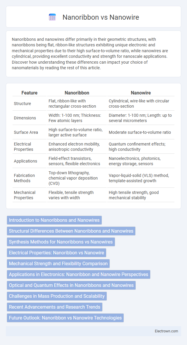
| Feature | Nanoribbon | Nanowire |
|---|---|---|
| Structure | Flat, ribbon-like with rectangular cross-section | Cylindrical, wire-like with circular cross-section |
| Dimensions | Width: 1-100 nm; Thickness: Few atomic layers | Diameter: 1-100 nm; Length: up to several micrometers |
| Surface Area | High surface-to-volume ratio, larger active surface | Moderate surface-to-volume ratio |
| Electrical Properties | Enhanced electron mobility, anisotropic conductivity | Quantum confinement effects; high conductivity |
| Applications | Field-effect transistors, sensors, flexible electronics | Nanoelectronics, photonics, energy storage, sensors |
| Fabrication Methods | Top-down lithography, chemical vapor deposition (CVD) | Vapor-liquid-solid (VLS) method, template-assisted growth |
| Mechanical Properties | Flexible, tensile strength varies with width | High tensile strength, good mechanical stability |
Introduction to Nanoribbons and Nanowires
Nanoribbons are ultra-thin, ribbon-shaped nanomaterials characterized by their high aspect ratio and unique edge properties, while nanowires are cylindrical nanostructures with diameters in the nanometer range and exceptional electrical and mechanical characteristics. Both nanoribbons and nanowires serve as fundamental building blocks in nanoscale devices, offering distinct advantages in electronics, photonics, and sensing applications due to their quantum confinement effects and enhanced surface area. Understanding the differences in geometry, synthesis methods, and electronic behavior of these nanostructures is crucial for optimizing their integration into your advanced nanotechnology projects.
Structural Differences Between Nanoribbons and Nanowires
Nanoribbons are thin, flat structures with a high aspect ratio, typically exhibiting a two-dimensional morphology, while nanowires possess a cylindrical shape with a uniform diameter along their length, representing a one-dimensional form. Nanoribbons have well-defined width and thickness, offering anisotropic properties distinct from the isotropic nature of nanowires. Your choice between nanoribbon and nanowire structures depends on the desired electronic, optical, and mechanical properties stemming from these fundamental structural differences.
Synthesis Methods for Nanoribbons vs Nanowires
Nanoribbons are primarily synthesized using bottom-up approaches like chemical vapor deposition (CVD) and molecular beam epitaxy (MBE), enabling precise control over width and thickness at the atomic scale. Nanowires are commonly produced through vapor-liquid-solid (VLS) growth and solution-phase synthesis, facilitating high aspect ratio structures with tunable diameters. Both techniques exploit different catalyst and substrate interactions to optimize crystal quality and dimensional uniformity for targeted applications in nanoelectronics and photonics.
Electrical Properties: Nanoribbon vs Nanowire
Nanoribbons exhibit superior electrical conductivity compared to nanowires due to their larger surface area and quantum confinement effects, which enable enhanced electron mobility. Nanowires often demonstrate higher resistance and limited electrical performance because of their smaller cross-sectional area and increased surface scattering. Understanding these differences allows you to optimize device designs for applications requiring efficient charge transport.
Mechanical Strength and Flexibility Comparison
Nanoribbons exhibit superior mechanical strength and flexibility compared to nanowires due to their two-dimensional geometry, which allows for better stress distribution and resistance to deformation. Nanowires, with their cylindrical structure, often experience higher brittleness under bending or tensile forces. Understanding these differences can help you select the optimal nanomaterial for applications requiring specific mechanical resilience and adaptability.
Applications in Electronics: Nanoribbon and Nanowire Perspectives
Nanoribbons offer enhanced surface area and edge states, making them ideal for high-performance field-effect transistors and flexible electronics, while nanowires excel in nanoscale interconnects and sensors due to their superior one-dimensional electron transport properties. Your choice between nanoribbons and nanowires depends on specific device requirements like conductivity, mechanical flexibility, and integration density. Both nanostructures push the boundaries of miniaturization and performance in next-generation electronic components.
Optical and Quantum Effects in Nanoribbons and Nanowires
Nanoribbons exhibit unique optical properties due to their anisotropic quantum confinement, leading to tunable band gaps and polarized light emission crucial for nanoscale photonic devices. In contrast, nanowires possess isotropic quantum confinement, resulting in discrete energy levels and enhanced exciton binding energies that improve charge carrier dynamics in quantum dot lasers. These distinct quantum and optical effects enable nanoribbons and nanowires to be tailored for applications in quantum computing, optoelectronics, and high-efficiency solar cells.
Challenges in Mass Production and Scalability
Nanoribbons and nanowires face significant challenges in mass production due to their precise dimensional control requirements and the need for uniformity at the nanoscale. Scaling up fabrication methods like chemical vapor deposition or lithography often leads to defects and variability, impacting the performance consistency of nanoscale devices. Your ability to implement cost-effective and scalable synthesis techniques determines the feasibility of integrating these nanomaterials into commercial applications.
Recent Advancements and Research Trends
Recent advancements in nanoribbons and nanowires emphasize their unique electrical, optical, and mechanical properties, driven by developments in synthesis techniques such as chemical vapor deposition and molecular beam epitaxy. Research trends highlight enhanced conductivity and flexibility in graphene nanoribbons compared to traditional semiconductor nanowires, making them promising for nanoelectronics and photonics applications. Your exploration of these nanostructures can benefit from ongoing studies that focus on scalable fabrication methods and integration into wearable and flexible electronic devices.
Future Outlook: Nanoribbon vs Nanowire Technologies
Nanoribbon and nanowire technologies present distinct advantages for future nanoelectronics, with nanoribbons offering superior mechanical flexibility and tunable electronic properties due to their planar geometry and edge effects. Nanowires excel in vertical integration and provide high surface-area-to-volume ratios, enhancing sensor performance and energy storage applications. Advancements in synthesis techniques and device integration are expected to drive the convergence of both nanostructures in next-generation flexible, high-performance electronic and photonic systems.
Nanoribbon vs Nanowire Infographic