2D materials exhibit unique electronic, optical, and mechanical properties due to their atomic thickness, contrasting sharply with bulk materials that have three-dimensional structures and different behavior. Explore the rest of the article to understand how these differences can impact your applications in electronics, energy storage, and beyond.
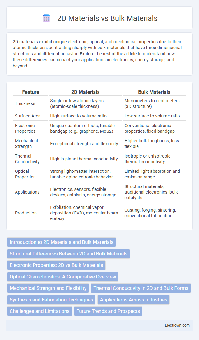
Table of Comparison
| Feature | 2D Materials | Bulk Materials |
|---|---|---|
| Thickness | Single or few atomic layers (atomic-scale thickness) | Micrometers to centimeters (3D structure) |
| Surface Area | High surface-to-volume ratio | Low surface-to-volume ratio |
| Electronic Properties | Unique quantum effects, tunable bandgap (e.g., graphene, MoS2) | Conventional electronic properties, fixed bandgap |
| Mechanical Strength | Exceptional strength and flexibility | Higher bulk toughness, less flexible |
| Thermal Conductivity | High in-plane thermal conductivity | Isotropic or anisotropic thermal conductivity |
| Optical Properties | Strong light-matter interaction, tunable optoelectronic behavior | Limited light absorption and emission range |
| Applications | Electronics, sensors, flexible devices, catalysis, energy storage | Structural materials, traditional electronics, bulk catalysts |
| Production | Exfoliation, chemical vapor deposition (CVD), molecular beam epitaxy | Casting, forging, sintering, conventional fabrication |
Introduction to 2D Materials and Bulk Materials
2D materials consist of a single or few atomic layers with exceptional electrical, mechanical, and thermal properties due to their reduced dimensionality, making them ideal for next-generation electronic and energy applications. Bulk materials, in contrast, have three-dimensional atomic arrangements that exhibit conventional properties influenced by their larger volume and surface area, widely used in structural and industrial applications. Your choice between 2D and bulk materials depends on the specific performance requirements and application scale.
Structural Differences Between 2D and Bulk Materials
2D materials consist of a single or few layers of atoms arranged in a flat plane, exhibiting strong in-plane covalent bonds and weak van der Waals forces between layers, contrasting with bulk materials that possess a three-dimensional interconnected atomic lattice. This structural difference leads to unique mechanical, electrical, and optical properties in 2D materials, such as higher surface area and quantum confinement effects absent in bulk counterparts. The reduced dimensionality in 2D materials results in anisotropy and enhanced tunability, making them ideal for applications in nanoelectronics and photonics compared to bulk materials.
Electronic Properties: 2D vs Bulk Materials
Two-dimensional (2D) materials exhibit unique electronic properties unlike their bulk counterparts due to quantum confinement and reduced dimensionality, leading to phenomena such as high electron mobility, tunable band gaps, and strong spin-orbit coupling. Bulk materials generally possess fixed band structures and lower electron mobility because of extensive atomic layering and three-dimensional interactions. In applications like transistors and sensors, 2D materials such as graphene and transition metal dichalcogenides outperform bulk materials through enhanced conductivity, greater flexibility, and controllable electronic band engineering.
Optical Characteristics: A Comparative Overview
2D materials exhibit unique optical characteristics such as strong light-matter interactions and tunable bandgaps due to their atomic-scale thickness, leading to enhanced photoluminescence and excitonic effects compared to bulk materials. Bulk materials generally have fixed optical properties governed by their three-dimensional crystal structures, resulting in lower absorption coefficients and less pronounced quantum confinement effects. These differences make 2D materials highly promising for applications in optoelectronics, photodetectors, and flexible displays.
Mechanical Strength and Flexibility
2D materials such as graphene exhibit exceptional mechanical strength with tensile strength surpassing bulk materials like steel, due to their strong covalent bonds within a single-atom-thick plane. Their atomic thinness grants superior flexibility, allowing bending and stretching without fracture, unlike bulk materials which are more prone to cracking under similar conditions. Your choice of 2D materials can enhance applications requiring lightweight, durable, and highly flexible components compared to traditional bulk alternatives.
Thermal Conductivity in 2D and Bulk Forms
2D materials such as graphene exhibit exceptionally high thermal conductivity, often surpassing their bulk counterparts due to the reduced phonon scattering in the atomically thin layers. Bulk materials generally have lower thermal conductivity because phonons encounter more scattering events from defects, grain boundaries, and three-dimensional lattice structures. The anisotropic thermal transport in 2D materials enables superior heat dissipation capabilities, making them ideal for advanced thermal management applications compared to traditional bulk materials.
Synthesis and Fabrication Techniques
2D materials are typically synthesized through methods like chemical vapor deposition (CVD), mechanical exfoliation, and molecular beam epitaxy (MBE), offering atomic-level control and uniform thin films. Bulk materials are commonly fabricated using traditional techniques such as melt growth, sintering, and casting, supporting larger-scale production but with less precision at the atomic scale. Your choice between 2D materials and bulk materials depends on the required application's performance criteria and fabrication complexity.
Applications Across Industries
2D materials like graphene and transition metal dichalcogenides revolutionize electronics, energy storage, and flexible devices due to their exceptional electrical conductivity, mechanical strength, and atomic thickness. Bulk materials, while traditionally used in construction, automotive, and aerospace industries, often lack the nanoscale properties essential for next-generation technologies but remain vital for structural applications. Your choice between 2D and bulk materials depends on the required performance characteristics and industry-specific demands for innovation and durability.
Challenges and Limitations
2D materials face challenges such as scalability in production, structural defects, and environmental instability that restrict their widespread industrial application compared to bulk materials. Bulk materials exhibit greater mechanical robustness and thermal stability but lack the unique electronic and optical properties inherent to atomically thin 2D structures. Limitations in interfacing 2D materials with existing technologies and difficulties in achieving uniform thickness further complicate their integration into commercial devices.
Future Trends and Prospects
2D materials, characterized by their atomic-scale thickness and exceptional mechanical, electrical, and optical properties, are poised to revolutionize future technologies such as flexible electronics, quantum computing, and energy storage. Bulk materials, while offering established performance and scalability, face limitations in miniaturization and efficiency that 2D materials can overcome through enhanced surface area and tunable band structures. Your exploration in material science could benefit from focusing on the integration of 2D materials in next-generation devices and the development of hybrid systems combining both 2D and bulk materials for optimized performance.
2D materials vs Bulk materials Infographic