Defect engineering involves intentionally introducing defects into materials to tailor their properties, while strain engineering focuses on applying mechanical deformation to alter electronic, optical, or mechanical behaviors. Discover how mastering these techniques can enhance your material design by exploring the detailed differences in the rest of this article.
Table of Comparison
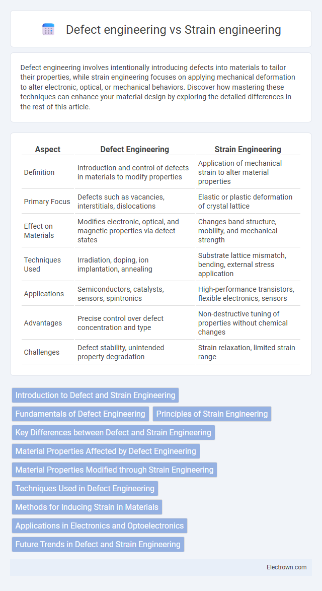
| Aspect | Defect Engineering | Strain Engineering |
|---|---|---|
| Definition | Introduction and control of defects in materials to modify properties | Application of mechanical strain to alter material properties |
| Primary Focus | Defects such as vacancies, interstitials, dislocations | Elastic or plastic deformation of crystal lattice |
| Effect on Materials | Modifies electronic, optical, and magnetic properties via defect states | Changes band structure, mobility, and mechanical strength |
| Techniques Used | Irradiation, doping, ion implantation, annealing | Substrate lattice mismatch, bending, external stress application |
| Applications | Semiconductors, catalysts, sensors, spintronics | High-performance transistors, flexible electronics, sensors |
| Advantages | Precise control over defect concentration and type | Non-destructive tuning of properties without chemical changes |
| Challenges | Defect stability, unintended property degradation | Strain relaxation, limited strain range |
Introduction to Defect and Strain Engineering
Defect engineering involves intentionally introducing or manipulating imperfections such as vacancies, interstitials, or dislocations within a material to alter its electrical, optical, or mechanical properties. Strain engineering focuses on applying or controlling mechanical deformation to modify lattice parameters, thereby tuning the electronic band structure and enhancing semiconductor device performance. Your choice between defect and strain engineering depends on the targeted material properties and application requirements.
Fundamentals of Defect Engineering
Defect engineering manipulates imperfections in materials at the atomic or nanoscale level to tailor electrical, optical, and mechanical properties for advanced device applications. It involves controlling vacancies, interstitials, and substitutional atoms to optimize carrier concentration, mobility, and recombination rates. Your ability to strategically introduce or mitigate defects influences material performance more directly than strain engineering, which relies on lattice distortion to affect band structure and mechanical stress.
Principles of Strain Engineering
Strain engineering involves deliberately altering the lattice structure of materials to modulate their electronic, optical, and mechanical properties by applying tensile or compressive stress. This technique enhances carrier mobility, bandgap tuning, and materials' performance in semiconductors, photovoltaics, and flexible electronics. Unlike defect engineering, which introduces imperfections to modify material behavior, strain engineering manipulates atomic spacing without creating lattice defects, enabling reversible and controllable property adjustments.
Key Differences between Defect and Strain Engineering
Defect engineering involves deliberately introducing or controlling imperfections, such as vacancies or interstitials, in a material's crystal lattice to modify its electrical, optical, or mechanical properties. Strain engineering manipulates the lattice structure by applying mechanical deformation to alter band structures or enhance carrier mobility without changing the material's chemical composition. You can leverage defect engineering for localized property tuning at the atomic level, while strain engineering is often employed to induce uniform changes across larger material areas.
Material Properties Affected by Defect Engineering
Defect engineering significantly alters material properties such as electrical conductivity, mechanical strength, and thermal stability by intentionally introducing vacancies, interstitials, or substitutional atoms to modify crystal structures. These defects create localized energy states that influence carrier concentration and mobility, enabling tailored semiconducting or catalytic behaviors. Your ability to control defect types and densities directly impacts device performance and material durability in applications ranging from electronics to energy storage.
Material Properties Modified through Strain Engineering
Strain engineering modifies material properties by altering the lattice structure, enabling precise control over electronic band gaps, carrier mobility, and optical responses in semiconductors. This technique enhances mechanical strength and flexibility, crucial for advanced flexible electronics and photonic devices. Your ability to tailor these properties through strain engineering surpasses defect engineering, which primarily introduces localized disruptions rather than systematic lattice alterations.
Techniques Used in Defect Engineering
Techniques used in defect engineering primarily involve ion implantation, thermal annealing, and plasma treatment to introduce or manipulate defects within a material's crystal lattice, thereby tailoring its electrical and mechanical properties. These methods create vacancies, interstitials, or substitutional defects, which can enhance conductivity, influence carrier concentration, or improve material strength. Your control over such defects is crucial for optimizing semiconductor devices and advanced materials for specific applications.
Methods for Inducing Strain in Materials
Defect engineering introduces controlled imperfections such as vacancies, interstitials, and dislocations to alter a material's properties, while strain engineering applies external mechanical forces or lattice mismatches to induce deformation at the atomic level. Methods for inducing strain include substrate-induced epitaxial growth, thermal expansion mismatches, and application of external stress via bending or stretching. Your choice depends on the desired material performance, with strain engineering often enabling tunable electronic and optical properties critical for semiconductor devices.
Applications in Electronics and Optoelectronics
Defect engineering enhances electronic and optoelectronic device performance by precisely controlling vacancy, interstitial, or substitutional defects to tailor charge carrier recombination and transport properties. Strain engineering modifies the electronic band structure and optical properties by applying mechanical deformation, enabling improved carrier mobility and tunable emission wavelengths in devices like transistors, LEDs, and photodetectors. Both techniques are crucial in optimizing semiconductor materials such as silicon, GaN, and transition metal dichalcogenides for high-efficiency sensors, solar cells, and flexible electronics.
Future Trends in Defect and Strain Engineering
Future trends in defect and strain engineering emphasize the integration of atomic-scale manipulation techniques to tailor material properties for next-generation electronic and quantum devices. Advances in machine learning-driven simulations are accelerating the prediction and control of defect configurations and strain distributions with unprecedented precision. Your ability to harness these innovations will drive breakthroughs in flexible electronics, energy storage, and nanoscale sensors.
Defect engineering vs Strain engineering Infographic