2D Crystal FETs offer superior electrostatic control and reduced short-channel effects compared to Bulk Crystal FETs, making them ideal for next-generation nanoelectronics. Explore the rest of the article to understand how these advancements can impact your semiconductor device applications.
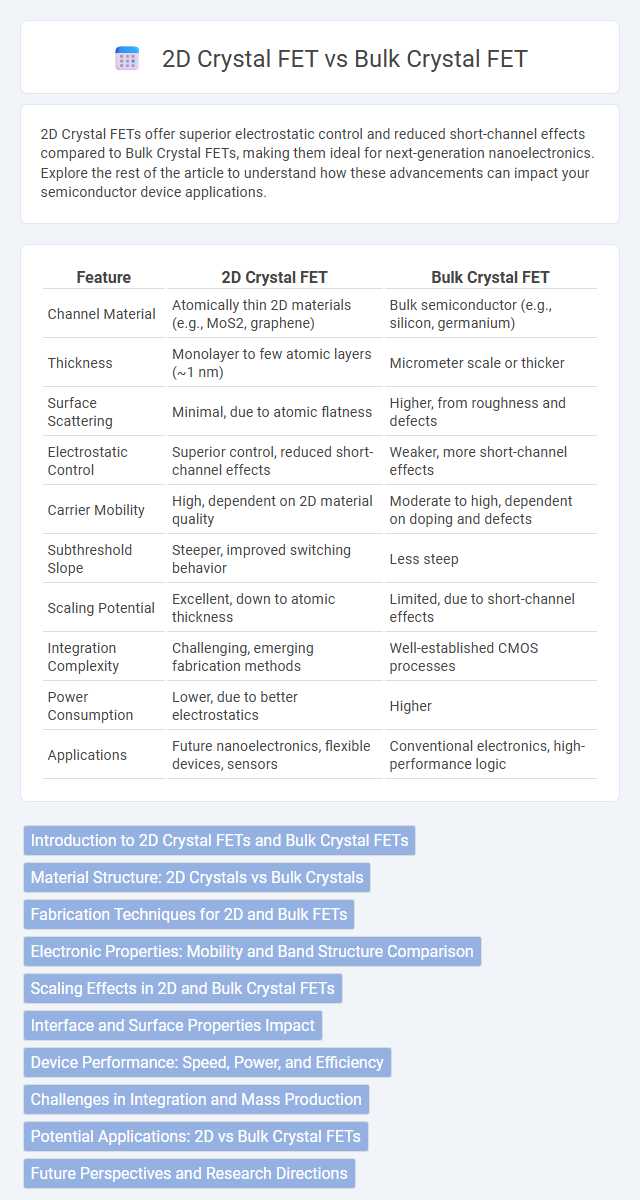
Table of Comparison
| Feature | 2D Crystal FET | Bulk Crystal FET |
|---|---|---|
| Channel Material | Atomically thin 2D materials (e.g., MoS2, graphene) | Bulk semiconductor (e.g., silicon, germanium) |
| Thickness | Monolayer to few atomic layers (~1 nm) | Micrometer scale or thicker |
| Surface Scattering | Minimal, due to atomic flatness | Higher, from roughness and defects |
| Electrostatic Control | Superior control, reduced short-channel effects | Weaker, more short-channel effects |
| Carrier Mobility | High, dependent on 2D material quality | Moderate to high, dependent on doping and defects |
| Subthreshold Slope | Steeper, improved switching behavior | Less steep |
| Scaling Potential | Excellent, down to atomic thickness | Limited, due to short-channel effects |
| Integration Complexity | Challenging, emerging fabrication methods | Well-established CMOS processes |
| Power Consumption | Lower, due to better electrostatics | Higher |
| Applications | Future nanoelectronics, flexible devices, sensors | Conventional electronics, high-performance logic |
Introduction to 2D Crystal FETs and Bulk Crystal FETs
2D Crystal FETs utilize atomically thin semiconductor layers like transition metal dichalcogenides, offering superior electrostatic control and scalability compared to traditional Bulk Crystal FETs, which rely on thicker, three-dimensional semiconductor substrates. The reduced thickness in 2D Crystal FETs minimizes short-channel effects and enables enhanced device performance at nanoscale dimensions. Understanding these differences is crucial for optimizing Your device design and achieving advancements in nanoelectronics technology.
Material Structure: 2D Crystals vs Bulk Crystals
2D Crystal FETs utilize atomically thin layers with a well-defined, planar structure that enables superior electrostatic control and reduced short-channel effects compared to bulk crystal FETs, which consist of thicker, three-dimensional semiconductor materials. The distinct layered arrangement in 2D crystals such as transition metal dichalcogenides (TMDs) offers enhanced carrier mobility and minimized surface defects, contrasting with the more defect-prone and volumetric nature of bulk crystals. Understanding this material structure difference helps optimize your device performance by leveraging the unique electrical and mechanical properties inherent to 2D materials.
Fabrication Techniques for 2D and Bulk FETs
2D Crystal FET fabrication involves atomic layer deposition and mechanical exfoliation methods to achieve ultra-thin channels with controlled thickness at the atomic scale, enhancing electron mobility and device performance. Bulk Crystal FETs typically use traditional bulk silicon wafer processing techniques such as photolithography and doping to form thicker, three-dimensional channels with well-established fabrication infrastructure. Your choice between 2D and bulk FET fabrication depends on desired device scaling, performance, and integration with existing semiconductor technologies.
Electronic Properties: Mobility and Band Structure Comparison
2D Crystal FETs exhibit significantly higher carrier mobility compared to Bulk Crystal FETs due to reduced scattering and enhanced electrostatic control in atomically thin layers. The band structure of 2D materials, such as transition metal dichalcogenides, enables direct bandgaps and tunable electronic properties, whereas bulk crystals typically have indirect bandgaps and less flexibility in band engineering. These intrinsic electronic advantages result in faster switching speeds and improved device performance for 2D Crystal FETs over their bulk counterparts.
Scaling Effects in 2D and Bulk Crystal FETs
Scaling effects in 2D Crystal FETs enable superior electrostatic control and reduced short-channel effects compared to Bulk Crystal FETs, due to their atomically thin channels. The ultra-thin body of 2D materials significantly suppresses drain-induced barrier lowering (DIBL) and improves subthreshold slope, enhancing device performance at nanometer scales. Your device can benefit from the enhanced scalability of 2D Crystal FETs, achieving higher drive currents and better energy efficiency in advanced technology nodes.
Interface and Surface Properties Impact
2D Crystal FETs exhibit superior interface properties due to their atomically flat and dangling-bond-free surfaces, minimizing interface trap density and enhancing carrier mobility compared to Bulk Crystal FETs. The absence of surface states in 2D materials significantly reduces scattering and charge trapping at the interface, leading to improved threshold voltage stability and reduced hysteresis. In contrast, Bulk Crystal FETs suffer from rougher surfaces and dangling bonds that increase interface defects, degrading device performance and reliability.
Device Performance: Speed, Power, and Efficiency
2D Crystal FETs exhibit significantly higher carrier mobility compared to Bulk Crystal FETs, resulting in faster switching speeds and enhanced overall device performance. The ultra-thin channel of 2D materials reduces short-channel effects and leakage currents, enabling lower power consumption and improved energy efficiency. Bulk Crystal FETs, constrained by thicker channels and higher defect densities, generally show slower speeds and increased power dissipation under similar operating conditions.
Challenges in Integration and Mass Production
2D Crystal FETs face significant challenges in integration and mass production due to the difficulty in uniform large-area synthesis and transfer processes, which affect device consistency and yield. Bulk Crystal FETs benefit from mature fabrication techniques and well-established substrates, enabling more reliable large-scale manufacturing but with limitations in scaling and performance. Your choice between these technologies depends on balancing the integration complexity of 2D materials with the proven manufacturability of bulk crystals.
Potential Applications: 2D vs Bulk Crystal FETs
2D Crystal FETs offer significant advantages in flexible electronics, high-frequency devices, and sensors due to their atomic-scale thickness and superior electrostatic control, enabling ultra-low power consumption and enhanced carrier mobility. Bulk Crystal FETs remain prevalent in traditional semiconductor applications such as microprocessors and power electronics, benefiting from established manufacturing processes and higher current drive capabilities. The unique properties of 2D materials position 2D Crystal FETs as key components in next-generation nanoelectronics, while Bulk Crystal FETs continue to dominate large-scale integrated circuits and commercial device fabrication.
Future Perspectives and Research Directions
2D Crystal FETs offer superior electrostatic control and scalability compared to Bulk Crystal FETs, making them promising candidates for next-generation nanoelectronics. Future research is focused on enhancing material synthesis, interface engineering, and contact optimization to overcome challenges like variability and stability. Your engagement in advancing 2D material integration could accelerate the development of ultra-low power, high-performance transistors for flexible and wearable devices.
2D Crystal FET vs Bulk Crystal FET Infographic