Atomic layer deposition provides precise, atomic-scale control over film thickness and uniformity, making it ideal for applications requiring ultra-thin, conformal coatings. Discover how these techniques differ and which one suits your specific needs by reading the rest of the article.
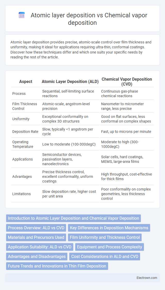
Table of Comparison
| Aspect | Atomic Layer Deposition (ALD) | Chemical Vapor Deposition (CVD) |
|---|---|---|
| Process | Sequential, self-limiting surface reactions | Continuous gas-phase chemical reactions |
| Film Thickness Control | Atomic-scale, angstrom-level precision | Nanometer to micrometer range, less precise |
| Uniformity | Exceptional conformality on complex 3D structures | Good on flat surfaces, less conformal on complex shapes |
| Deposition Rate | Slow, typically <1 angstrom per cycle | Fast, up to microns per minute |
| Operating Temperature | Low to moderate (100-300degC) | Moderate to high (300-1000degC) |
| Applications | Semiconductor devices, passivation layers, nanoelectronics | Solar cells, hard coatings, MEMS, large-area films |
| Advantages | Precise thickness control, excellent conformality, uniform coatings | High throughput, cost-effective for thick films |
| Limitations | Slow deposition rate, higher cost per unit area | Poor conformality on complex geometries, less thickness control |
Introduction to Atomic Layer Deposition and Chemical Vapor Deposition
Atomic Layer Deposition (ALD) is a thin film deposition technique characterized by sequential, self-limiting surface reactions that enable atomic-scale thickness control and conformality on complex substrate geometries. Chemical Vapor Deposition (CVD) involves continuous chemical reactions of gaseous precursors on heated substrates, producing high-purity, uniform films over large areas rapidly. ALD excels in precision and uniformity for nanoscale applications, while CVD is widely used in large-scale semiconductor fabrication and coating processes requiring high throughput.
Process Overview: ALD vs CVD
Atomic layer deposition (ALD) is a vapor phase technique that deposits thin films one atomic layer at a time through sequential, self-limiting surface reactions, ensuring precise thickness control and uniformity. Chemical vapor deposition (CVD) involves continuous chemical reactions of gaseous precursors on a heated substrate, producing thicker films at higher deposition rates but with less atomic-level precision. ALD's stepwise approach contrasts with CVD's steady-state mechanism, making ALD ideal for ultrathin, conformal coatings and CVD suitable for thicker, faster film growth.
Key Differences in Deposition Mechanisms
Atomic layer deposition (ALD) relies on sequential, self-limiting surface reactions that deposit materials one atomic layer at a time, ensuring exceptional thickness control and conformality over complex structures. Chemical vapor deposition (CVD) involves continuous chemical reactions of gaseous precursors on a heated substrate, resulting in faster deposition rates but less precise thickness control compared to ALD. You should choose ALD for applications requiring precise nanoscale film uniformity, while CVD suits high-throughput coatings where speed is prioritized.
Materials and Precursors Used
Atomic layer deposition (ALD) typically uses highly reactive precursors such as metal-organic compounds and halides, allowing precise control over ultra-thin film growth at the atomic level, mainly for oxides, nitrides, and sulfides. Chemical vapor deposition (CVD) employs a broader range of materials including silanes, hydrocarbons, and metal-organic chemicals, enabling the deposition of thicker films like silicon dioxide, silicon nitride, and diamond-like carbon. Your choice between ALD and CVD depends on the desired material composition and film thickness, as ALD offers superior conformality and uniformity with self-limiting surface reactions, whereas CVD provides faster deposition rates with diverse precursor options.
Film Uniformity and Thickness Control
Atomic layer deposition (ALD) offers superior film uniformity and atomic-scale thickness control due to its self-limiting surface reactions, enabling conformal coatings even on complex 3D structures. Chemical vapor deposition (CVD) typically results in faster deposition rates but can produce less uniform films with thickness variations, especially on high-aspect-ratio features. ALD is preferred in applications requiring precise thickness control and uniformity, such as in semiconductor device fabrication and advanced nanotechnology.
Application Suitability: ALD vs CVD
Atomic Layer Deposition (ALD) offers superior control and uniformity for ultra-thin films, making it ideal for advanced semiconductor devices and nanotechnology applications. Chemical Vapor Deposition (CVD) is better suited for high-throughput manufacturing where thicker films and rapid deposition are required, such as in solar panels and hard coatings. Your choice between ALD and CVD should depend on the specific film thickness precision and application scale needed.
Equipment and Process Complexity
Atomic layer deposition (ALD) requires highly specialized equipment with precise control over precursor exposure and purge cycles to achieve atomic-scale film thickness uniformity, resulting in greater process complexity compared to chemical vapor deposition (CVD). CVD systems typically involve simpler reactor designs and continuous gas flow, allowing faster deposition rates but less precise thickness control. Your choice between ALD and CVD depends on whether equipment sophistication and ultra-thin film accuracy or faster throughput and simpler process setup are your primary priorities.
Advantages and Disadvantages
Atomic layer deposition (ALD) offers unparalleled control over film thickness and uniformity at the atomic scale, making it ideal for ultra-thin and conformal coatings on complex substrates, though it typically exhibits slower deposition rates and higher process complexity compared to chemical vapor deposition (CVD). Chemical vapor deposition provides faster growth rates and is well-suited for large-scale production with a wide range of materials, but it may suffer from less precise thickness control and non-uniform coatings on high-aspect-ratio structures. Trade-offs between ALD and CVD often center on precision versus throughput, where ALD excels in nanoscale accuracy while CVD dominates in scalability and material versatility.
Cost Considerations in ALD and CVD
Atomic layer deposition (ALD) often incurs higher costs due to its slower deposition rates and precise, layer-by-layer growth, which demands specialized equipment and controlled environments. Chemical vapor deposition (CVD) generally offers more cost-effective scaling for larger-area coatings and faster throughput but may lead to less uniform films compared to ALD. The choice between ALD and CVD balances capital investment, operational expenses, and film quality requirements specific to semiconductor manufacturing or advanced material applications.
Future Trends and Innovations in Thin Film Deposition
Atomic layer deposition (ALD) and chemical vapor deposition (CVD) are evolving with innovations like plasma-enhanced processes and low-temperature techniques to enhance film uniformity and conformality in advanced semiconductor manufacturing. Future trends emphasize integrating ALD's atomic precision with CVD's high throughput for next-generation optoelectronics and flexible electronics applications. Your choice between ALD and CVD will increasingly depend on the balance between film quality, scalability, and application-specific requirements driven by these technological advancements.
Atomic layer deposition vs Chemical vapor deposition Infographic