Doped nanocrystals exhibit enhanced electrical and optical properties compared to undoped nanocrystals, making them more effective in applications such as sensors and photodetectors. Discover how these differences can impact your choice by reading the rest of the article.
Table of Comparison
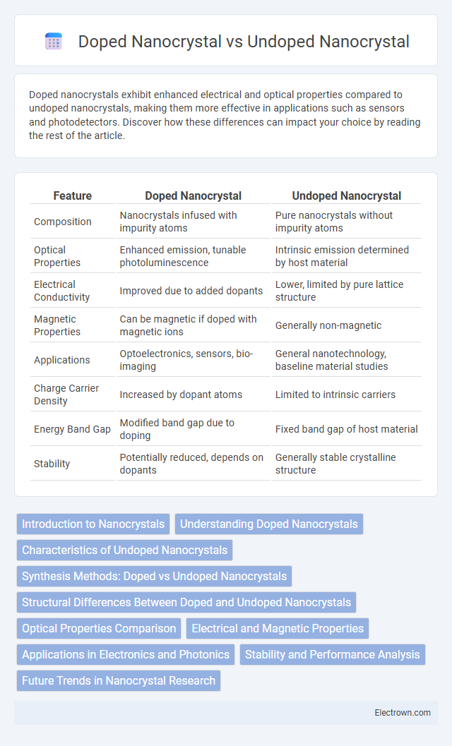
| Feature | Doped Nanocrystal | Undoped Nanocrystal |
|---|---|---|
| Composition | Nanocrystals infused with impurity atoms | Pure nanocrystals without impurity atoms |
| Optical Properties | Enhanced emission, tunable photoluminescence | Intrinsic emission determined by host material |
| Electrical Conductivity | Improved due to added dopants | Lower, limited by pure lattice structure |
| Magnetic Properties | Can be magnetic if doped with magnetic ions | Generally non-magnetic |
| Applications | Optoelectronics, sensors, bio-imaging | General nanotechnology, baseline material studies |
| Charge Carrier Density | Increased by dopant atoms | Limited to intrinsic carriers |
| Energy Band Gap | Modified band gap due to doping | Fixed band gap of host material |
| Stability | Potentially reduced, depends on dopants | Generally stable crystalline structure |
Introduction to Nanocrystals
Nanocrystals are crystalline particles with dimensions typically below 100 nanometers, exhibiting unique optical and electronic properties due to quantum confinement effects. Doped nanocrystals contain intentional impurities introduced to modify electrical, magnetic, or optical characteristics, enhancing functionality for applications like LEDs, sensors, or solar cells. Undoped nanocrystals lack these dopants, displaying intrinsic properties primarily influenced by size, shape, and composition, serving as a baseline for comparative studies in nanomaterial research.
Understanding Doped Nanocrystals
Doped nanocrystals incorporate impurity atoms into their crystal lattice, altering electrical, optical, and magnetic properties compared to undoped nanocrystals, which maintain their pure material structures. These dopants introduce localized energy states within the bandgap, enabling enhanced functionality for applications in optoelectronics, photovoltaics, and bioimaging. Understanding the precise control over dopant concentration and distribution is crucial for optimizing performance and tailoring nanocrystal behavior in advanced nanotechnology devices.
Characteristics of Undoped Nanocrystals
Undoped nanocrystals exhibit intrinsic properties dictated by their pure semiconductor material, including size-dependent optical absorption and emission that arise from quantum confinement effects. These nanocrystals typically show high photoluminescence quantum yields and sharp emission peaks due to their uniform electronic band structures. Your applications can benefit from the stable and reproducible optical and electronic behavior of undoped nanocrystals, which lack impurity-induced trap states found in doped counterparts.
Synthesis Methods: Doped vs Undoped Nanocrystals
Synthesis methods for doped nanocrystals involve the incorporation of impurity atoms into the host crystal lattice during nucleation or growth, typically achieved through co-precipitation, thermal decomposition, or solvothermal processes with controlled dopant concentration. Undoped nanocrystals are synthesized primarily via simpler methods like colloidal synthesis, hot-injection, or hydrothermal routes without the addition of dopant precursors. Precise control over temperature, reaction time, and precursor ratios is critical in doped nanocrystals to ensure uniform dopant distribution and desired physicochemical properties, unlike undoped nanocrystals which focus mainly on size and shape control.
Structural Differences Between Doped and Undoped Nanocrystals
Doped nanocrystals exhibit altered lattice structures due to the intentional incorporation of impurity atoms, which can introduce lattice strain or defects compared to undoped nanocrystals with pristine, uniform crystal lattices. These structural modifications affect electronic, optical, and magnetic properties by changing bond lengths, coordination environments, and local symmetry within the crystal matrix. Understanding these differences enables you to tailor material properties for applications in photovoltaics, sensors, and optoelectronic devices.
Optical Properties Comparison
Doped nanocrystals exhibit enhanced optical properties compared to undoped nanocrystals, such as increased photoluminescence intensity and tunable emission wavelengths due to the incorporation of impurity ions. The presence of dopants creates localized energy states that facilitate efficient radiative recombination, resulting in sharper and more stable emission spectra. In contrast, undoped nanocrystals typically show broader emission bands with less control over wavelength specificity and lower quantum yields.
Electrical and Magnetic Properties
Doped nanocrystals exhibit enhanced electrical conductivity and tunable magnetic properties due to the introduction of impurity atoms that create additional charge carriers and magnetic moments. In contrast, undoped nanocrystals typically have lower electrical conductivity and lack significant magnetic behavior because their intrinsic properties dominate without external impurities. The controlled doping of nanocrystals enables precise manipulation of charge transport and magnetic responses, making them suitable for advanced applications in spintronics and nanoelectronics.
Applications in Electronics and Photonics
Doped nanocrystals exhibit enhanced electronic conductivity and tunable optical properties, making them ideal for applications in light-emitting diodes, photodetectors, and quantum dot solar cells. Undoped nanocrystals maintain intrinsic electronic and photonic characteristics, useful in biological imaging and basic semiconductor research. The controlled introduction of dopants enables precise manipulation of charge carriers and emission spectra, expanding the functional versatility of nanocrystals in advanced electronic and photonic devices.
Stability and Performance Analysis
Doped nanocrystals exhibit superior stability and enhanced performance compared to undoped nanocrystals due to the intentional introduction of impurity atoms that modulate electronic and optical properties. This doping improves charge carrier mobility, reduces defect-induced recombination, and increases resistance to environmental degradation. Understanding these differences allows you to optimize nanocrystal applications in fields such as optoelectronics and photovoltaics.
Future Trends in Nanocrystal Research
Doped nanocrystals exhibit enhanced optical and electronic properties compared to undoped nanocrystals, enabling advancements in quantum dot displays, photodetectors, and solar cells. Future trends in nanocrystal research emphasize precise doping techniques to control charge carriers and magnetic properties, driving innovations in spintronics and bioimaging. Emerging studies also focus on scalable synthesis methods and environmental stability to facilitate commercial applications of doped nanocrystals.
Doped Nanocrystal vs Undoped Nanocrystal Infographic