Top-down fabrication involves etching or milling bulk materials to create nanostructures, offering precise control but often resulting in higher waste and cost, whereas bottom-up fabrication builds structures atom-by-atom or molecule-by-molecule, enabling more efficient material use and potentially superior nanoscale customization. Discover how these methods impact your project's design and performance by reading the rest of the article.
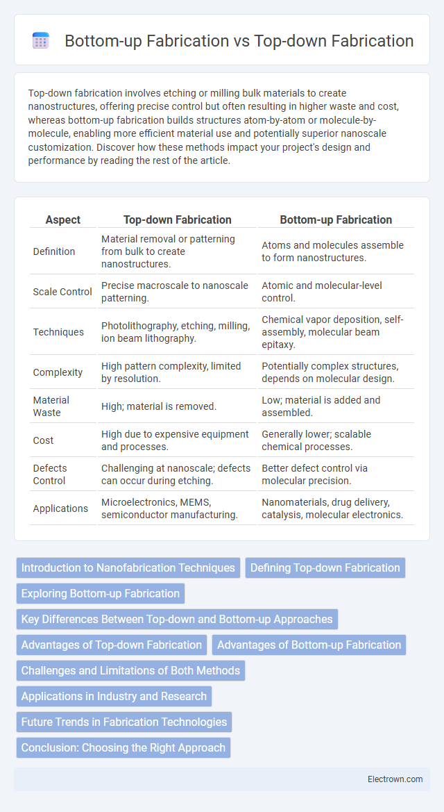
Table of Comparison
| Aspect | Top-down Fabrication | Bottom-up Fabrication |
|---|---|---|
| Definition | Material removal or patterning from bulk to create nanostructures. | Atoms and molecules assemble to form nanostructures. |
| Scale Control | Precise macroscale to nanoscale patterning. | Atomic and molecular-level control. |
| Techniques | Photolithography, etching, milling, ion beam lithography. | Chemical vapor deposition, self-assembly, molecular beam epitaxy. |
| Complexity | High pattern complexity, limited by resolution. | Potentially complex structures, depends on molecular design. |
| Material Waste | High; material is removed. | Low; material is added and assembled. |
| Cost | High due to expensive equipment and processes. | Generally lower; scalable chemical processes. |
| Defects Control | Challenging at nanoscale; defects can occur during etching. | Better defect control via molecular precision. |
| Applications | Microelectronics, MEMS, semiconductor manufacturing. | Nanomaterials, drug delivery, catalysis, molecular electronics. |
Introduction to Nanofabrication Techniques
Nanofabrication techniques encompass top-down and bottom-up fabrication methods essential for creating nanoscale structures. Top-down fabrication involves patterning and etching bulk materials to sculpt nanostructures, commonly used in semiconductor manufacturing with techniques like photolithography and electron beam lithography. Bottom-up fabrication relies on assembling atoms or molecules through chemical synthesis or self-assembly processes, enabling precise control over nanoscale features in applications such as quantum dots and molecular electronics.
Defining Top-down Fabrication
Top-down fabrication involves the process of creating nanoscale structures by starting with bulk materials and etching or patterning them down to the desired size and shape, often using techniques such as photolithography or electron beam lithography. This method provides precise control over dimensions and is widely used in semiconductor manufacturing for integrated circuits. Despite its accuracy, top-down fabrication can be limited by material waste and difficulty in achieving atomic-scale precision compared to bottom-up approaches.
Exploring Bottom-up Fabrication
Bottom-up fabrication involves assembling materials at the atomic or molecular level, enabling precise control over nanostructures and improved material properties. This approach facilitates the creation of complex nanodevices by self-assembly and chemical synthesis, often resulting in higher efficiency and scalability compared to traditional top-down methods. Advances in bottom-up fabrication techniques, such as atomic layer deposition and molecular beam epitaxy, are driving innovations in electronics, photonics, and biotechnology.
Key Differences Between Top-down and Bottom-up Approaches
Top-down fabrication involves the systematic removal or patterning of material from larger bulk structures to create nanoscale features, typically using techniques like lithography and etching. Bottom-up fabrication builds structures atom-by-atom or molecule-by-molecule through self-assembly, chemical synthesis, or deposition processes, enabling precise control at the atomic scale. Key differences include scalability, with top-down suited for mass production but limited in atomic precision, while bottom-up offers superior nanoscale accuracy but faces challenges in uniformity and large-scale manufacturing.
Advantages of Top-down Fabrication
Top-down fabrication offers precise control over device geometry and uniformity, making it ideal for creating complex micro- and nanoscale structures with high reproducibility. This method allows for easy integration with existing manufacturing processes and materials, reducing development time and costs. Your projects benefit from the scalability and reliability of top-down techniques, especially in semiconductor and microelectronics production.
Advantages of Bottom-up Fabrication
Bottom-up fabrication offers precise control at the atomic or molecular level, enabling the creation of complex nanostructures with superior uniformity and fewer defects compared to top-down methods. This approach allows for cost-effective manufacturing by reducing material waste and energy consumption during the synthesis process. Your ability to tailor materials from the ground up enhances the performance and functionality of nanoscale devices in applications like electronics, medicine, and energy storage.
Challenges and Limitations of Both Methods
Top-down fabrication faces challenges such as high production costs, limited resolution due to lithography constraints, and material wastage during etching processes. Bottom-up fabrication is often limited by difficulties in controlling particle assembly at the nanoscale, potential defects in self-assembled structures, and scalability issues for industrial applications. Both methods struggle with reproducibility and integration into existing manufacturing systems, affecting their commercial viability.
Applications in Industry and Research
Top-down fabrication techniques, such as photolithography and etching, are widely used in semiconductor manufacturing for producing microchips with high precision and scalability, making them essential in electronics and MEMS industries. Bottom-up fabrication, including chemical vapor deposition and self-assembly, enables the creation of nanomaterials and molecular structures with atomic-level control, which is critical for advanced research in nanotechnology, drug delivery, and materials science. Your choice between these methods depends on the desired scale, complexity, and application area, balancing mass production capabilities with innovative material design.
Future Trends in Fabrication Technologies
Future trends in fabrication technologies emphasize the integration of top-down and bottom-up approaches to achieve higher precision and scalability in nanomanufacturing. Advances in atomic layer deposition, electron beam lithography, and self-assembly techniques are driving the development of hybrid fabrication processes that enhance device performance and reduce production costs. Emerging applications in flexible electronics, quantum computing, and biotechnology rely on these innovative methods to create complex nanostructures with unparalleled control at the atomic scale.
Conclusion: Choosing the Right Approach
Choosing the right fabrication approach depends on the required precision and scale of your project; top-down fabrication excels in creating well-defined microstructures, while bottom-up fabrication offers superior atomic-level control and material customization. Your specific application dictates whether the established methods of top-down lithography or the innovative assembly techniques of bottom-up synthesis will deliver optimal results. Balancing cost, complexity, and desired outcomes ensures that you select the most efficient fabrication method for advanced nanotechnology and materials engineering.
Top-down Fabrication vs Bottom-up Fabrication Infographic