Atomically thin materials consist of a few atomic layers, while monolayer materials are composed of exactly one atomic layer, resulting in distinct electronic and optical properties. Explore the rest of the article to understand how these differences impact your applications in nanotechnology and materials science.
Table of Comparison
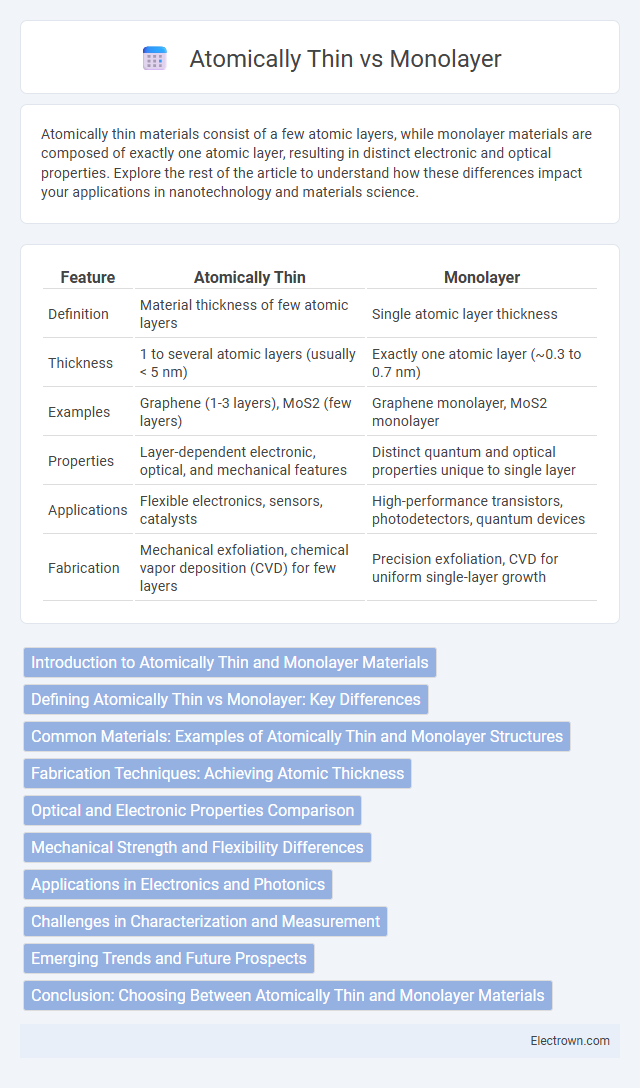
| Feature | Atomically Thin | Monolayer |
|---|---|---|
| Definition | Material thickness of few atomic layers | Single atomic layer thickness |
| Thickness | 1 to several atomic layers (usually < 5 nm) | Exactly one atomic layer (~0.3 to 0.7 nm) |
| Examples | Graphene (1-3 layers), MoS2 (few layers) | Graphene monolayer, MoS2 monolayer |
| Properties | Layer-dependent electronic, optical, and mechanical features | Distinct quantum and optical properties unique to single layer |
| Applications | Flexible electronics, sensors, catalysts | High-performance transistors, photodetectors, quantum devices |
| Fabrication | Mechanical exfoliation, chemical vapor deposition (CVD) for few layers | Precision exfoliation, CVD for uniform single-layer growth |
Introduction to Atomically Thin and Monolayer Materials
Atomically thin materials refer to substances composed of just a few atomic layers, offering exceptional electronic, optical, and mechanical properties. Monolayer materials are a subset of atomically thin materials consisting of a single atomic layer, which maximizes surface area and quantum effects. Your exploration of these materials is crucial for advancements in nanotechnology and flexible electronics.
Defining Atomically Thin vs Monolayer: Key Differences
Atomically thin materials consist of just a few atomic layers, whereas monolayers specifically refer to a single, continuous layer of atoms or molecules. The primary difference lies in thickness, with monolayers representing the ultimate thin limit of one atomic layer, while atomically thin can include multiple but still minimal atomic layers. This distinction is critical in nanomaterials research, where electronic, optical, and mechanical properties vary significantly between monolayer and few-layer atomically thin structures.
Common Materials: Examples of Atomically Thin and Monolayer Structures
Graphene and molybdenum disulfide (MoS2) are quintessential examples of atomically thin materials known for their single-atom or single-molecule thickness. Monolayer structures specifically refer to a single layer of atoms or molecules, commonly seen in materials like hexagonal boron nitride (h-BN) and transition metal dichalcogenides (TMDs) such as WS2 and MoSe2. Understanding these materials enhances your ability to explore advanced applications in electronics and nanotechnology, where precise material thickness at the atomic scale is crucial.
Fabrication Techniques: Achieving Atomic Thickness
Fabrication techniques for atomically thin and monolayer materials primarily include mechanical exfoliation, chemical vapor deposition (CVD), and molecular beam epitaxy (MBE), each ensuring precise control over atomic thickness. Mechanical exfoliation produces high-quality monolayers by peeling layers from bulk crystals, while CVD enables scalable production of uniform atomically thin films on diverse substrates. MBE offers atomic-level precision in thickness and composition, critical for electronic and optoelectronic applications requiring defect-free monolayer structures.
Optical and Electronic Properties Comparison
Atomically thin materials consist of single to few atomic layers, while monolayers specifically refer to a single atomic layer. Monolayers exhibit unique optical properties such as direct bandgap emissions, enhancing photoluminescence, whereas atomically thin materials may show indirect bandgap behavior with reduced optical efficiency. Your choice between monolayer and atomically thin materials significantly influences electronic performance in devices, with monolayers offering superior charge carrier mobility and tunable electronic properties.
Mechanical Strength and Flexibility Differences
Atomically thin materials, such as graphene, exhibit exceptional mechanical strength due to their single-atom thickness and strong covalent bonding, offering superior tensile strength compared to thicker counterparts. Monolayer structures, often composed of a single layer of atoms or molecules, combine high flexibility with remarkable durability, allowing them to bend and stretch without breaking. Understanding the differences in mechanical strength and flexibility between atomically thin and monolayer materials can help you select the right nanomaterial for applications requiring both resilience and adaptability.
Applications in Electronics and Photonics
Atomically thin materials consist of one or few atomic layers, whereas monolayers specifically refer to a single atomic layer with uniform thickness. In electronics, monolayer semiconductors like MoS2 offer superior charge mobility and tunable bandgaps ideal for transistors and flexible devices. Photonics applications leverage atomically thin materials for high-performance modulators, photodetectors, and light-emitting devices due to their strong light-matter interactions and quantum confinement effects.
Challenges in Characterization and Measurement
Atomically thin and monolayer materials present significant challenges in characterization and measurement due to their nanoscale thickness and sensitivity to environmental factors. Techniques such as atomic force microscopy (AFM) and Raman spectroscopy require precise calibration to accurately distinguish between a single monolayer and multiple atomic layers. Proper characterization of your material is crucial for ensuring reliable performance in applications like electronics and optoelectronics.
Emerging Trends and Future Prospects
Emerging trends in atomically thin and monolayer materials highlight their expanding role in flexible electronics, optoelectronics, and quantum computing due to unique electronic, optical, and mechanical properties. Research advances in transition metal dichalcogenides (TMDs) and graphene enable precise control over thickness at the atomic scale, improving device performance and enabling novel applications such as ultra-sensitive sensors and energy-efficient transistors. Future prospects emphasize scalable synthesis techniques, integration with existing semiconductor technologies, and exploration of heterostructures for multifunctional devices, driving innovation in next-generation nanotechnology platforms.
Conclusion: Choosing Between Atomically Thin and Monolayer Materials
Atomically thin materials refer to structures with thicknesses on the scale of a few atomic layers, while monolayer materials are exactly one atom thick. Choosing between atomically thin and monolayer materials depends on the specific application requirements such as electronic, optical, and mechanical properties, where monolayers often provide superior performance due to their uniform atomic thickness. For applications demanding precise quantum behaviors or maximum transparency, monolayers are preferred, whereas atomically thin materials offer flexibility in tuning properties by adjusting the number of layers.
Atomically thin vs Monolayer Infographic