At the nanoscale, Schottky diodes exhibit faster switching speeds and lower forward voltage drops compared to PN diodes due to their metal-semiconductor junction, which enhances electron mobility and reduces recombination. Explore the article to understand how these differences impact your nanoscale device performance in detail.
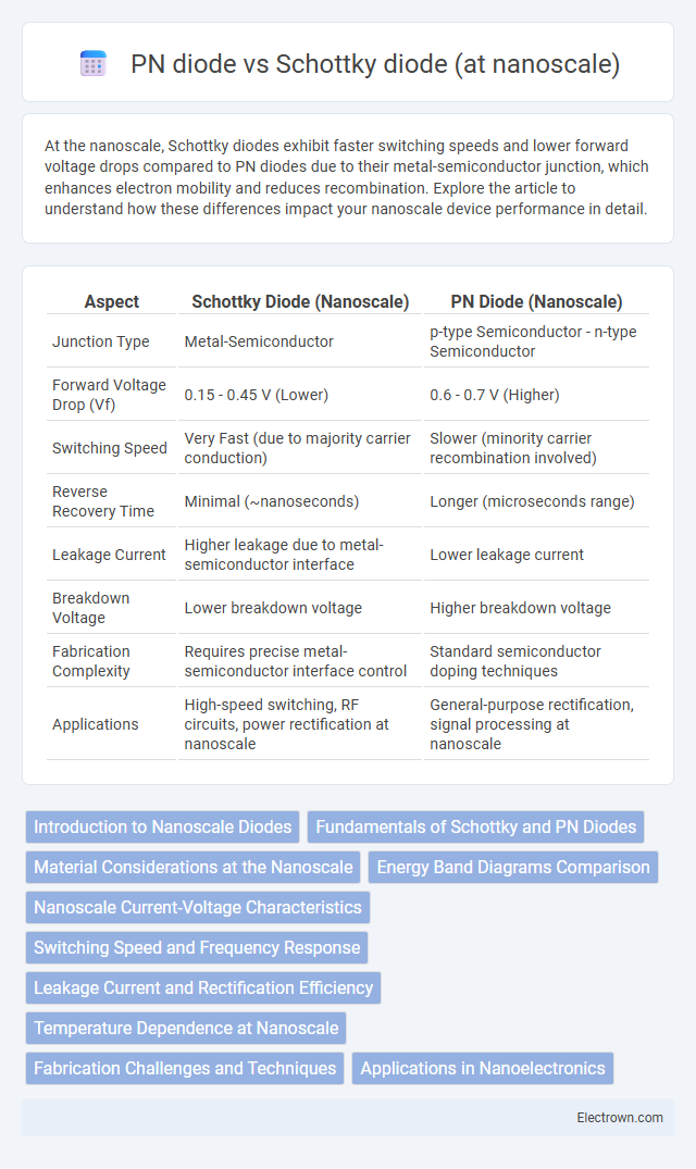
Table of Comparison
| Aspect | Schottky Diode (Nanoscale) | PN Diode (Nanoscale) |
|---|---|---|
| Junction Type | Metal-Semiconductor | p-type Semiconductor - n-type Semiconductor |
| Forward Voltage Drop (Vf) | 0.15 - 0.45 V (Lower) | 0.6 - 0.7 V (Higher) |
| Switching Speed | Very Fast (due to majority carrier conduction) | Slower (minority carrier recombination involved) |
| Reverse Recovery Time | Minimal (~nanoseconds) | Longer (microseconds range) |
| Leakage Current | Higher leakage due to metal-semiconductor interface | Lower leakage current |
| Breakdown Voltage | Lower breakdown voltage | Higher breakdown voltage |
| Fabrication Complexity | Requires precise metal-semiconductor interface control | Standard semiconductor doping techniques |
| Applications | High-speed switching, RF circuits, power rectification at nanoscale | General-purpose rectification, signal processing at nanoscale |
Introduction to Nanoscale Diodes
Nanoscale diodes, including Schottky and PN diodes, exhibit distinct electronic behaviors due to quantum confinement and interface effects at atomic dimensions. Schottky diodes leverage metal-semiconductor junctions, offering faster switching speeds and lower forward voltage drops compared to PN diodes, which rely on p-n junctions formed by doping. At the nanoscale, your choice between these diodes impacts device performance factors like current leakage, response time, and integration density in nanoelectronic circuits.
Fundamentals of Schottky and PN Diodes
Schottky diodes consist of a metal-semiconductor junction that enables fast switching and low forward voltage drop, whereas PN diodes are formed by joining p-type and n-type semiconductors creating a depletion region responsible for their rectifying behavior. At the nanoscale, Schottky diodes exhibit reduced junction capacitance and enhanced electron mobility due to quantum confinement effects, while PN diodes rely on diffusion and recombination processes within the atomic-scale depletion region. The fundamental difference lies in the Schottky barrier height determined by metal work function and semiconductor electron affinity, contrasting with the built-in potential governed by doping concentrations in PN diodes.
Material Considerations at the Nanoscale
At the nanoscale, Schottky diodes leverage metal-semiconductor junctions typically using materials like platinum or gold on silicon or gallium arsenide to achieve lower forward voltage drops and faster switching speeds compared to PN diodes. PN diodes rely on doping control within semiconductor crystals such as silicon or germanium, where precise atomic-scale modifications influence junction properties but introduce higher series resistance and slower response times. Your selection between Schottky and PN diodes at this scale hinges on material compatibility, interface quality, and the trade-offs between conductivity and breakdown voltage critical for nanoscale device performance.
Energy Band Diagrams Comparison
Schottky diodes at the nanoscale exhibit a metal-semiconductor junction with a lower barrier height in their energy band diagrams, resulting in minimal energy band bending and faster carrier transport compared to PN diodes. PN diodes display a p-n junction characterized by a pronounced depletion region and significant band bending, which increases the built-in potential and affects carrier recombination rates. Your choice depends on the required switching speed and voltage thresholds, with Schottky diodes offering superior performance in high-speed, low-voltage nanoscale applications.
Nanoscale Current-Voltage Characteristics
Nanoscale Schottky diodes exhibit lower forward voltage drops and faster switching speeds compared to PN diodes due to their metal-semiconductor junctions, which reduce carrier recombination and enhance electron transport. The current-voltage characteristics of Schottky diodes at the nanoscale show a more linear and abrupt turn-on behavior, resulting in higher on-state currents and reduced power losses. Understanding these differences is crucial for optimizing Your nanoscale electronic devices for improved efficiency and performance.
Switching Speed and Frequency Response
Schottky diodes exhibit significantly faster switching speeds and superior frequency response compared to PN diodes at the nanoscale due to their metal-semiconductor junction, which eliminates minority carrier charge storage. This results in low forward voltage drops and minimal reverse recovery time, enabling efficient operation in high-frequency applications such as RF circuits and high-speed switching devices. Optimizing Your nanoscale devices with Schottky diodes enhances performance in GHz frequency ranges and reduces power losses during rapid switching cycles.
Leakage Current and Rectification Efficiency
Schottky diodes at the nanoscale exhibit lower leakage current compared to PN diodes due to their metal-semiconductor junction, which reduces minority carrier injection and enables faster switching. The rectification efficiency of nanoscale Schottky diodes is generally higher as a result of their lower forward voltage drop and minimal charge storage effects, enhancing overall device performance. Your nanoscale applications benefit from choosing Schottky diodes when minimizing leakage current and maximizing rectification efficiency is critical.
Temperature Dependence at Nanoscale
At the nanoscale, Schottky diodes exhibit lower temperature dependence compared to PN diodes due to their metal-semiconductor junction, which results in reduced carrier recombination and enhanced thermal stability. Your device's performance can benefit from the Schottky diode's lower forward voltage drop and minimal leakage current variations over temperature changes. Conversely, PN diodes at nanoscale show significant shifts in threshold voltage and increased leakage with temperature due to intrinsic carrier generation in the depletion region.
Fabrication Challenges and Techniques
Fabricating Schottky diodes at the nanoscale requires precise control over metal-semiconductor interfaces to minimize defects and achieve low barrier heights, often utilizing techniques such as electron beam lithography and atomic layer deposition. In contrast, nanoscale PN diodes face challenges in achieving abrupt junctions and dopant precision, typically employing ion implantation combined with rapid thermal annealing to optimize dopant activation. Your choice depends on balancing these fabrication complexities with desired electrical performance, as Schottky diodes offer faster switching but demand superior interface quality compared to PN diodes.
Applications in Nanoelectronics
Schottky diodes at the nanoscale offer faster switching speeds and lower forward voltage drops than traditional PN diodes, making them ideal for high-frequency nanoelectronic circuits and ultrafast signal detection. Nanostructured Schottky diodes enable enhanced electron transport with reduced recombination, which significantly improves the efficiency of nano-scale rectifiers and transistors in integrated circuits. Your choice of diode impacts the performance of nanoelectronic devices where speed, power consumption, and miniaturization are critical.
Schottky diode vs PN diode (at nanoscale) Infographic