Band-to-band tunneling involves electrons directly transitioning between the valence band and conduction band across a semiconductor junction, significantly influencing leakage currents in devices like tunnel diodes. Understanding the differences between band-to-band tunneling and direct tunneling can help you optimize semiconductor device performance; explore the full article to learn more about these tunneling mechanisms.
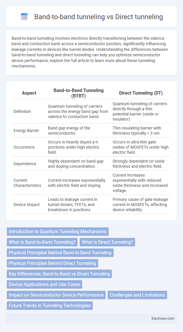
Table of Comparison
| Aspect | Band-to-Band Tunneling (BTBT) | Direct Tunneling (DT) |
|---|---|---|
| Definition | Quantum tunneling of carriers across the energy band gap from valence to conduction band. | Quantum tunneling of carriers directly through a thin potential barrier (oxide or insulator). |
| Energy Barrier | Band gap energy of the semiconductor. | Thin insulating barrier with thickness typically < 3 nm. |
| Occurrence | Occurs in heavily doped p-n junctions under high electric field. | Occurs in ultra-thin gate oxides of MOSFETs under high electric field. |
| Dependence | Highly dependent on band gap and doping concentration. | Strongly dependent on oxide thickness and electric field. |
| Current Characteristics | Current increases exponentially with electric field and doping. | Current increases exponentially with reduced oxide thickness and increased voltage. |
| Device Impact | Leads to leakage current in tunnel diodes, TFETs, and breakdown in junctions. | Primary cause of gate leakage current in MOSFETs, affecting device reliability. |
Introduction to Quantum Tunneling Mechanisms
Quantum tunneling mechanisms include band-to-band tunneling (BTBT) and direct tunneling, each characterized by distinct electron movement across potential barriers. BTBT involves electrons tunneling between the valence band of a semiconductor and its conduction band, often observed in heavily doped p-n junctions and critical for tunnel diodes and advanced MOSFETs. Your understanding of these mechanisms helps in optimizing semiconductor device performance by addressing leakage currents and switching speeds effectively.
What is Band-to-Band Tunneling?
Band-to-band tunneling (BTBT) is a quantum mechanical process where electrons tunnel directly from the valence band of a semiconductor to its conduction band, bypassing the forbidden energy gap. This phenomenon typically occurs under strong electric fields in heavily doped p-n junctions or tunnel diodes, enabling current flow at lower voltages. BTBT contrasts with direct tunneling, which involves electron tunneling through a thin insulating barrier rather than across the energy bands of a semiconductor.
What is Direct Tunneling?
Direct tunneling is a quantum mechanical process where electrons pass through an energy barrier by penetrating its potential barrier without occupying any intermediate energy states. This phenomenon typically occurs in ultrathin insulating layers, such as gate oxides in MOSFETs, allowing electrons to tunnel directly between the conduction bands of the semiconductor and the metal. It differs from band-to-band tunneling, which involves electrons transitioning across the bandgap from the valence band to the conduction band, often requiring a high electric field to facilitate the process.
Physical Principles Behind Band-to-Band Tunneling
Band-to-band tunneling occurs when electrons quantum mechanically tunnel between the valence band of the p-type material and the conduction band of the n-type material, bypassing the forbidden energy gap. This phenomenon relies on a strong electric field that narrows the energy barrier, allowing carriers to directly tunnel through the semiconductor bandgap. Understanding the physical principles behind band-to-band tunneling helps optimize device performance in applications such as tunnel diodes and advanced MOSFETs.
Physical Principles Behind Direct Tunneling
Direct tunneling occurs when electrons quantum-mechanically penetrate a thin energy barrier without requiring thermal activation, heavily influenced by the barrier's thickness and height. This tunneling involves electron wavefunction overlap across the insulating layer, enabling charge transport even at low voltages. Unlike band-to-band tunneling, which involves interband electron transitions in semiconductor junctions, direct tunneling primarily depends on the physical parameters of the oxide layer and the electron's tunneling probability.
Key Differences: Band-to-Band vs Direct Tunneling
Band-to-band tunneling occurs when electrons tunnel directly from the valence band to the conduction band across a narrow energy gap, common in tunnel diodes and certain semiconductor devices. Direct tunneling involves electrons passing through a thin energy barrier without energy band transition, often observed in MOSFET gate leakage currents. Your understanding of these mechanisms is crucial for optimizing device performance, as band-to-band tunneling impacts high electric field regions differently compared to the thickness-sensitive direct tunneling.
Device Applications and Use Cases
Band-to-band tunneling (BTBT) is predominantly utilized in tunnel field-effect transistors (TFETs) for ultra-low-power applications, offering steep subthreshold slopes ideal for energy-efficient logic devices. Direct tunneling, common in ultra-thin gate oxides of MOSFETs, plays a critical role in scaling down devices and is a key consideration in memory technologies like flash storage due to leakage currents. Your choice between these tunneling mechanisms impacts device performance, power consumption, and suitability for advanced semiconductor applications.
Impact on Semiconductor Device Performance
Band-to-band tunneling in semiconductor devices leads to increased leakage currents, especially under high electric fields, significantly affecting power efficiency and device reliability. Direct tunneling dominates in ultra-thin gate oxides, causing gate leakage that degrades threshold voltage stability and reduces device lifespan. Understanding the distinct tunneling mechanisms allows you to optimize device design for improved performance and minimized power loss.
Challenges and Limitations
Band-to-band tunneling faces challenges such as high electric field requirements and limited tunneling current control, restricting its efficiency in ultra-scaled devices. Direct tunneling is limited by oxide thickness scaling, where excessively thin barriers increase leakage currents, impacting device reliability and power consumption. Both tunneling mechanisms present integration difficulties in semiconductor technologies, demanding advanced material engineering to optimize performance while minimizing unwanted leakage.
Future Trends in Tunneling Technologies
Future trends in tunneling technologies emphasize enhanced efficiency and scalability for both band-to-band tunneling (BTBT) and direct tunneling mechanisms, enabling ultra-low power consumption in next-generation semiconductor devices. Innovations in material science, such as two-dimensional materials and high-k dielectrics, facilitate improved control over tunneling barriers, optimizing electron transport and minimizing leakage currents. Emerging applications in tunnel field-effect transistors (TFETs) and nanoscale transistors leverage these advancements to achieve higher switching speeds and energy-efficient performance at reduced device dimensions.
Band-to-band tunneling vs Direct tunneling Infographic