Plasmonic circuits use surface plasmons to transmit signals at optical frequencies, enabling faster data transfer and smaller device sizes compared to traditional electronic circuits that rely on electron flow in conductors. Explore the rest of the article to understand how plasmonic technology could revolutionize your future electronic devices.
Table of Comparison
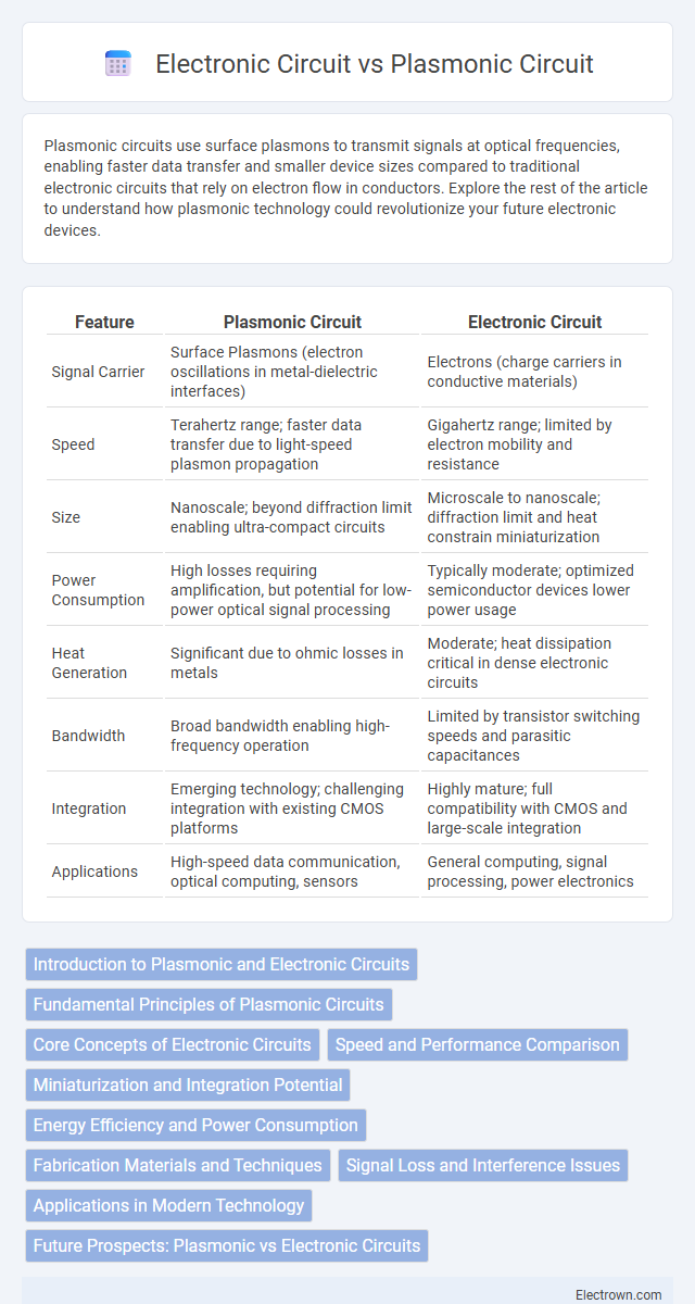
| Feature | Plasmonic Circuit | Electronic Circuit |
|---|---|---|
| Signal Carrier | Surface Plasmons (electron oscillations in metal-dielectric interfaces) | Electrons (charge carriers in conductive materials) |
| Speed | Terahertz range; faster data transfer due to light-speed plasmon propagation | Gigahertz range; limited by electron mobility and resistance |
| Size | Nanoscale; beyond diffraction limit enabling ultra-compact circuits | Microscale to nanoscale; diffraction limit and heat constrain miniaturization |
| Power Consumption | High losses requiring amplification, but potential for low-power optical signal processing | Typically moderate; optimized semiconductor devices lower power usage |
| Heat Generation | Significant due to ohmic losses in metals | Moderate; heat dissipation critical in dense electronic circuits |
| Bandwidth | Broad bandwidth enabling high-frequency operation | Limited by transistor switching speeds and parasitic capacitances |
| Integration | Emerging technology; challenging integration with existing CMOS platforms | Highly mature; full compatibility with CMOS and large-scale integration |
| Applications | High-speed data communication, optical computing, sensors | General computing, signal processing, power electronics |
Introduction to Plasmonic and Electronic Circuits
Plasmonic circuits exploit surface plasmon polaritons to enable light manipulation at the nanoscale, offering faster data transmission and higher bandwidth compared to traditional electronic circuits, which rely on electron flow through conductive materials. Electronic circuits dominate current technology due to their mature fabrication processes and effective voltage control but face limitations in speed and miniaturization caused by resistance and capacitance. Plasmonic circuits promise breakthroughs in photonic integration and ultrafast signal processing, merging optical and electronic functionalities for next-generation computing and communication systems.
Fundamental Principles of Plasmonic Circuits
Plasmonic circuits leverage surface plasmon polaritons--electromagnetic waves coupled with electron oscillations at metal-dielectric interfaces--to transmit signals at nanoscales with light-like speed and optical frequencies. Unlike electronic circuits that rely on electron flow through conductive materials and suffer from resistive losses and heat generation, plasmonic circuits utilize confinement of electromagnetic fields beyond the diffraction limit, enabling ultrafast data processing and miniaturized device integration. Key components in plasmonic circuits include waveguides, resonators, and modulators engineered to manipulate plasmon propagation with high sensitivity and tunability for applications in communication and sensing technologies.
Core Concepts of Electronic Circuits
Electronic circuits rely on the flow of electrons through conductive materials like copper wires, utilizing components such as resistors, capacitors, and transistors to control and manipulate electrical signals. These circuits operate based on voltage, current, and resistance principles governed by Ohm's Law and Kirchhoff's Laws, enabling signal processing, amplification, and switching. The fundamental mechanism involves charge carrier movement in semiconductor devices, which contrasts with plasmonic circuits that leverage surface plasmon resonances for signal transmission at optical frequencies.
Speed and Performance Comparison
Plasmonic circuits operate at the speed of light, offering significantly higher bandwidth and faster signal transmission than traditional electronic circuits, which are limited by electron mobility and resistive losses. The performance of plasmonic circuits excels in data processing and communication applications due to reduced latency and enhanced signal integrity at nanoscale dimensions. Your technology choices can benefit from the ultra-fast response times of plasmonic circuits when seeking improvements in speed and overall system performance.
Miniaturization and Integration Potential
Plasmonic circuits offer significantly greater miniaturization than traditional electronic circuits by enabling light manipulation at the nanoscale, far below the diffraction limit of conventional photonics. Their integration potential with existing semiconductor technologies facilitates the development of ultra-compact, high-speed data processing devices, overcoming the size and speed limitations of electronic components. By incorporating plasmonic elements, your circuits can achieve enhanced performance and scalability suitable for next-generation nanoscale communication systems.
Energy Efficiency and Power Consumption
Plasmonic circuits exhibit significantly higher energy efficiency compared to traditional electronic circuits due to their ability to manipulate light at the nanoscale, minimizing resistive losses and heat generation. In contrast, electronic circuits suffer from increased power consumption caused by electron scattering and Joule heating in conductive materials. This fundamental difference enables plasmonic circuits to offer lower power consumption while supporting faster data transmission rates, making them ideal for next-generation energy-efficient computing devices.
Fabrication Materials and Techniques
Plasmonic circuits primarily utilize noble metals such as gold and silver, fabricated through advanced nanolithography techniques including electron beam lithography and focused ion beam milling, enabling subwavelength plasmon confinement. Electronic circuits rely on semiconductor materials like silicon and gallium arsenide, produced using well-established photolithography, chemical vapor deposition (CVD), and doping processes optimized for electron mobility. The fabrication of plasmonic devices demands higher precision at the nanoscale to control surface plasmon resonance, whereas electronic circuits focus on material purity and layer uniformity to enhance electrical conductivity and transistor performance.
Signal Loss and Interference Issues
Plasmonic circuits experience lower signal loss due to their ability to confine light at the nanoscale, which reduces energy dissipation compared to electronic circuits relying on electron flow in conductors. Electronic circuits often face significant interference issues from electromagnetic noise, causing signal degradation, whereas plasmonic circuits offer improved resistance to such noise due to their optical nature. Understanding these differences can help optimize your circuit design for higher efficiency and reduced interference in advanced communication systems.
Applications in Modern Technology
Plasmonic circuits enable ultrafast data transmission and enhanced signal processing in optical communication systems, surpassing electronic circuits in bandwidth and speed. Electronic circuits remain dominant in traditional computing and power management due to their mature manufacturing processes and energy efficiency. Integrating plasmonic components with electronic circuits paves the way for hybrid devices used in photonic computing, biosensing, and high-frequency wireless communication.
Future Prospects: Plasmonic vs Electronic Circuits
Plasmonic circuits offer significantly higher data processing speeds and bandwidths than traditional electronic circuits due to their ability to manipulate light at nanoscale dimensions. Future prospects indicate plasmonics could revolutionize on-chip communication and sensing technologies by overcoming electronic circuits' limitations in heat dissipation and signal delay. Integrating plasmonic components with conventional electronics may lead to hybrid systems that maximize performance for advanced computing and telecommunications.
Plasmonic Circuit vs Electronic Circuit Infographic