Sputter deposition creates thin films by ejecting material from a target onto a substrate through ion bombardment, offering rapid coverage and good adhesion. Atomic layer deposition provides precise, atomic-scale thickness control by sequentially exposing the substrate to gas-phase precursors, ideal for uniform coatings on complex structures; explore the rest of the article to understand which technique best suits your application needs.
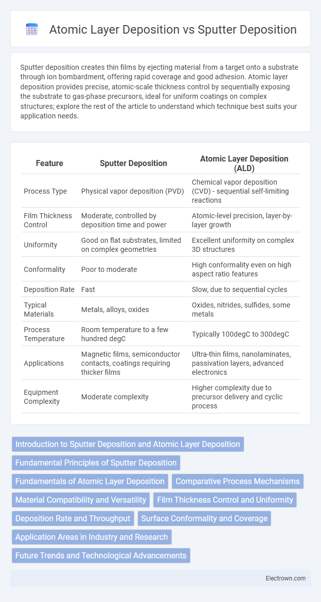
Table of Comparison
| Feature | Sputter Deposition | Atomic Layer Deposition (ALD) |
|---|---|---|
| Process Type | Physical vapor deposition (PVD) | Chemical vapor deposition (CVD) - sequential self-limiting reactions |
| Film Thickness Control | Moderate, controlled by deposition time and power | Atomic-level precision, layer-by-layer growth |
| Uniformity | Good on flat substrates, limited on complex geometries | Excellent uniformity on complex 3D structures |
| Conformality | Poor to moderate | High conformality even on high aspect ratio features |
| Deposition Rate | Fast | Slow, due to sequential cycles |
| Typical Materials | Metals, alloys, oxides | Oxides, nitrides, sulfides, some metals |
| Process Temperature | Room temperature to a few hundred degC | Typically 100degC to 300degC |
| Applications | Magnetic films, semiconductor contacts, coatings requiring thicker films | Ultra-thin films, nanolaminates, passivation layers, advanced electronics |
| Equipment Complexity | Moderate complexity | Higher complexity due to precursor delivery and cyclic process |
Introduction to Sputter Deposition and Atomic Layer Deposition
Sputter deposition utilizes energetic ions to eject atoms from a target material, enabling thin film growth with high uniformity and good adhesion, ideal for metals and alloys. Atomic layer deposition (ALD) relies on sequential, self-limiting surface reactions to build films atom-by-atom, offering exceptional thickness control and conformality on complex 3D substrates. Understanding these deposition methods helps you select the best technique for precise thin film applications in semiconductor manufacturing and advanced coatings.
Fundamental Principles of Sputter Deposition
Sputter deposition relies on the physical ejection of atoms from a target material by bombarding it with high-energy ions, typically in a plasma environment. This process enables the coating of substrates with thin films through the direct transfer of material, offering excellent control over film uniformity and thickness. Your choice between sputter deposition and atomic layer deposition depends on the desired film quality, thickness precision, and application requirements.
Fundamentals of Atomic Layer Deposition
Atomic Layer Deposition (ALD) is a precise thin film deposition technique that relies on sequential self-limiting surface reactions to achieve atomic-scale thickness control, essential for uniform and conformal coatings on complex substrates. Unlike Sputter Deposition, which uses physical bombardment to deposit material, ALD's chemical process enables excellent film uniformity even on high aspect ratio structures. Your choice of ALD allows for superior thickness control and material quality in semiconductor, nanotechnology, and coating applications.
Comparative Process Mechanisms
Sputter Deposition utilizes physical vapor deposition by bombarding a target material with high-energy ions, causing atoms to eject and condense onto a substrate, enabling rapid, uniform thin film formation. Atomic Layer Deposition (ALD) relies on sequential, self-limiting chemical reactions between gaseous precursors and the substrate surface, offering unparalleled atomic-scale thickness control and conformality. Your choice depends on the required precision, film uniformity, and deposition rate, with sputtering favoring speed and ALD excelling in nanoscale layer accuracy.
Material Compatibility and Versatility
Sputter deposition supports a wide range of materials including metals, alloys, and oxides, providing versatility for complex, multi-layer coatings on diverse substrates such as semiconductors and polymers. Atomic layer deposition excels in conformal thin films with atomic-scale thickness control, particularly for high-k dielectrics and metal oxides on 3D nanostructures, ensuring uniformity on high-aspect-ratio surfaces. Material compatibility in ALD involves self-limiting surface reactions suitable for delicate and temperature-sensitive substrates, contrasting with the kinetic sputtering process used in sputter deposition.
Film Thickness Control and Uniformity
Sputter deposition offers moderate film thickness control with deposition rates typically ranging from 0.1 to 10 nm per minute, achieving uniformity within 3-5% over large substrates. Atomic layer deposition (ALD) provides atomic-scale thickness control with single monolayer precision, resulting in exceptional uniformity often better than 1% across complex 3D structures. Due to ALD's self-limiting surface reactions, it ensures conformal coatings even on high-aspect-ratio features, surpassing sputtering in uniformity and thickness consistency.
Deposition Rate and Throughput
Sputter deposition typically features higher deposition rates and throughput, making it suitable for large-area coatings and industrial-scale production. Atomic layer deposition (ALD), while offering unmatched film conformality and thickness control, operates at significantly lower deposition rates, resulting in reduced throughput. Your choice depends on the balance between speed and precision required for the application, with sputtering favoring rapid material deposition and ALD excelling in uniform atomic-scale layers.
Surface Conformality and Coverage
Sputter deposition offers moderate surface conformality but may struggle with uniform coverage on complex, high-aspect-ratio structures due to its line-of-sight nature. Atomic layer deposition (ALD) excels in surface conformality and provides unparalleled uniform coverage, even on intricate 3D nanostructures, by utilizing self-limiting chemical reactions. Your choice between these techniques should consider the required precision in conformality and coverage for advanced semiconductor or coating applications.
Application Areas in Industry and Research
Sputter deposition is widely utilized in semiconductor manufacturing, data storage devices, and optical coatings due to its ability to deposit thin metallic and alloy films with high uniformity over large areas. Atomic layer deposition (ALD) excels in producing ultra-thin, conformal coatings for microelectronics, energy storage devices, and nanotechnology research, enabling precise thickness control at the atomic scale. Both techniques are critical in catalysis and sensor development, with sputter deposition favoring large-scale industrial production and ALD facilitating advanced research requiring nanoscale film control.
Future Trends and Technological Advancements
Sputter deposition and atomic layer deposition (ALD) are advancing rapidly with trends focusing on enhanced precision and scalability for semiconductor and nanotechnology applications. Innovations in ALD now enable ultra-thin, conformal coatings with atomic-level control, critical for next-generation electronics and energy devices, while sputter deposition is evolving to support larger substrates and complex material compositions. Your choice between these methods will increasingly depend on the need for atomic-scale uniformity versus throughput and material versatility as both technologies integrate AI-driven process controls and novel plasma sources.
Sputter Deposition vs Atomic Layer Deposition Infographic