Monolayer graphene exhibits exceptional electrical conductivity and mechanical strength due to its single atomic layer structure, while few-layer graphene offers enhanced stability and easier handling with slightly altered electronic properties. Discover how these differences impact your applications and why choosing the right type of graphene matters by reading the full article.
Table of Comparison
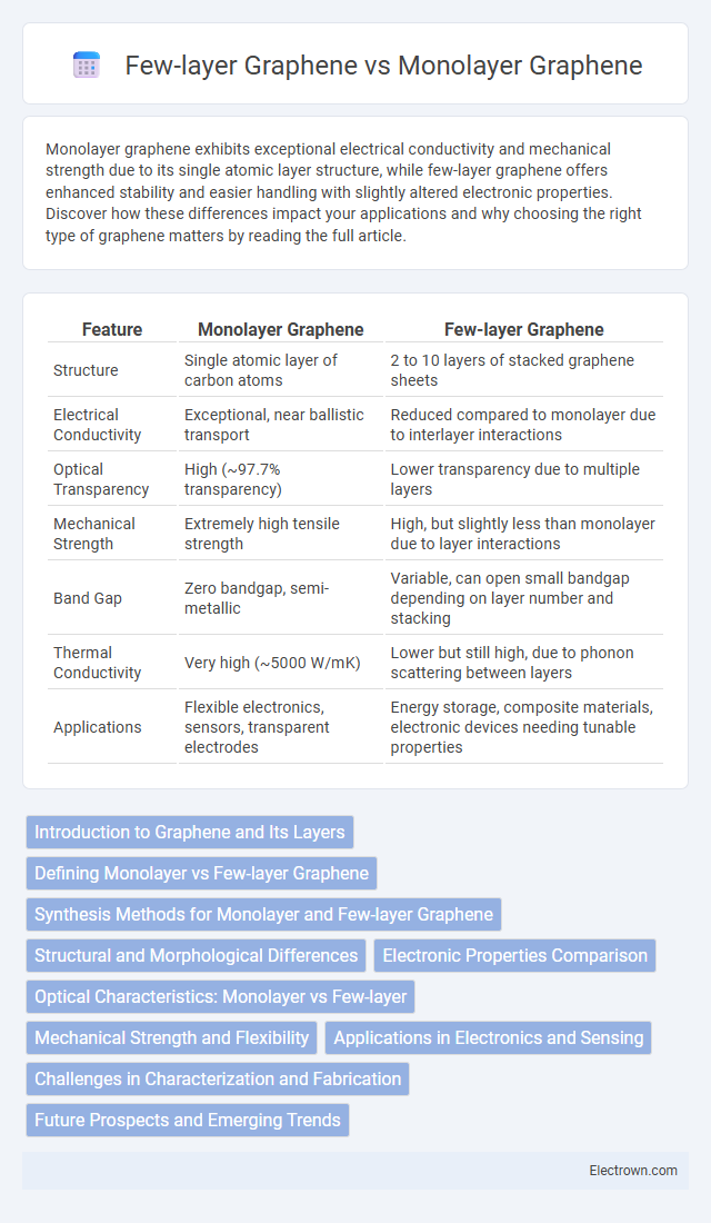
| Feature | Monolayer Graphene | Few-layer Graphene |
|---|---|---|
| Structure | Single atomic layer of carbon atoms | 2 to 10 layers of stacked graphene sheets |
| Electrical Conductivity | Exceptional, near ballistic transport | Reduced compared to monolayer due to interlayer interactions |
| Optical Transparency | High (~97.7% transparency) | Lower transparency due to multiple layers |
| Mechanical Strength | Extremely high tensile strength | High, but slightly less than monolayer due to layer interactions |
| Band Gap | Zero bandgap, semi-metallic | Variable, can open small bandgap depending on layer number and stacking |
| Thermal Conductivity | Very high (~5000 W/mK) | Lower but still high, due to phonon scattering between layers |
| Applications | Flexible electronics, sensors, transparent electrodes | Energy storage, composite materials, electronic devices needing tunable properties |
Introduction to Graphene and Its Layers
Graphene is a two-dimensional material composed of a single layer of carbon atoms arranged in a hexagonal lattice, offering exceptional electrical, thermal, and mechanical properties. Monolayer graphene consists of one atomic layer, providing high electron mobility and transparency, while few-layer graphene comprises two to five layers, enhancing mechanical strength and altering electronic band structure. Differences in layer number significantly influence graphene's applications in electronics, sensors, and composite materials due to varying conductivity and optical characteristics.
Defining Monolayer vs Few-layer Graphene
Monolayer graphene consists of a single sheet of carbon atoms arranged in a two-dimensional honeycomb lattice, exhibiting exceptional electrical conductivity and mechanical strength due to its atomic thickness. Few-layer graphene comprises two to ten atomic layers stacked via van der Waals forces, displaying altered electronic properties such as tunable band gaps and enhanced optical absorption compared to monolayer graphene. The distinction between monolayer and few-layer graphene significantly impacts their applications in nanoelectronics, sensors, and composite materials.
Synthesis Methods for Monolayer and Few-layer Graphene
Monolayer graphene is commonly synthesized using chemical vapor deposition (CVD) on copper substrates, which promotes single-layer growth due to the low carbon solubility in copper. Few-layer graphene is often produced via mechanical exfoliation, liquid-phase exfoliation, or CVD on nickel substrates, where higher carbon solubility enables multilayer formation. Epitaxial growth on silicon carbide is another method that can yield both monolayer and few-layer graphene depending on decomposition conditions and substrate orientation.
Structural and Morphological Differences
Monolayer graphene consists of a single atomic layer of carbon atoms arranged in a hexagonal lattice, resulting in exceptional electrical conductivity and mechanical strength due to its two-dimensional structure. Few-layer graphene comprises multiple stacked graphene sheets, typically ranging from two to five layers, which introduces interlayer interactions that modify its electronic properties and increase thickness. Morphologically, monolayer graphene is atomically thin and transparent, while few-layer graphene exhibits greater opacity and enhanced stability from van der Waals forces between layers.
Electronic Properties Comparison
Monolayer graphene exhibits exceptional electronic properties characterized by a zero bandgap and massless Dirac fermions, resulting in high electron mobility and quantum Hall effects. Few-layer graphene introduces interlayer interactions that modify its band structure, often opening a small bandgap and altering charge carrier dynamics, which can reduce mobility compared to monolayer graphene. Your choice between monolayer and few-layer graphene depends on whether ultra-high conductivity or tunable electronic properties are prioritized for specific applications.
Optical Characteristics: Monolayer vs Few-layer
Monolayer graphene exhibits exceptional optical transparency, absorbing approximately 2.3% of visible light per atomic layer, making it nearly invisible and ideal for transparent conductive applications. Few-layer graphene, on the other hand, shows increased light absorption and reduced transparency due to the cumulative effect of multiple layers, which also leads to altered optical conductivity and plasmonic properties. Your choice between monolayer and few-layer graphene depends on the specific optical performance requirements in devices such as photodetectors, sensors, or transparent electrodes.
Mechanical Strength and Flexibility
Monolayer graphene exhibits exceptional mechanical strength with a tensile strength of approximately 130 GPa and Young's modulus near 1 TPa, offering remarkable stiffness and flexibility at the atomic scale. Few-layer graphene, while slightly less strong due to interlayer interactions, provides enhanced flexibility and improved mechanical stability for practical applications, balancing robustness and pliability. The layer-dependent van der Waals forces in few-layer graphene influence its deformation behavior, making it suitable for flexible electronics and composite materials.
Applications in Electronics and Sensing
Monolayer graphene offers exceptional electron mobility and transparency, making it ideal for high-frequency transistors and flexible transparent electrodes in advanced electronics. Few-layer graphene, with tunable bandgap and enhanced mechanical strength, is better suited for robust sensors and energy storage devices requiring higher durability and sensitivity. You can leverage monolayer graphene for ultra-fast electronic components, while few-layer graphene enhances performance in chemical and biological sensing applications.
Challenges in Characterization and Fabrication
Monolayer graphene presents significant challenges in fabrication due to its extreme thinness and sensitivity to environmental factors, often requiring precise control of temperature and substrate interactions during growth processes like chemical vapor deposition (CVD). Characterization techniques need to overcome limitations in spatial resolution and susceptibility to contaminants, with tools such as Raman spectroscopy and atomic force microscopy (AFM) playing critical roles but sometimes yielding ambiguous data for defect identification. Few-layer graphene, while easier to fabricate with more robust mechanical properties, complicates characterization as layer stacking and interlayer interactions affect electronic properties, necessitating advanced techniques like transmission electron microscopy (TEM) for accurate layer number determination and defect analysis.
Future Prospects and Emerging Trends
Monolayer graphene exhibits exceptional electrical conductivity and mechanical strength, making it ideal for high-performance nanoelectronics and flexible devices, while few-layer graphene offers enhanced stability and tunable bandgap properties critical for energy storage and sensor applications. Emerging trends focus on hybrid structures combining monolayer and few-layer graphene to leverage synergistic effects for advanced optoelectronics and quantum computing. Future prospects include scalable production methods and integration with 2D materials to drive innovations in wearable technology, photonics, and sustainable energy solutions.
Monolayer Graphene vs Few-layer Graphene Infographic