Dielectric breakdown occurs when an insulating material suddenly becomes conductive under high electric fields, while quantum tunneling allows particles to pass through energy barriers at the quantum level despite classical restrictions. Discover how these distinct phenomena impact modern electronics and what it means for your device design in the rest of this article.
Table of Comparison
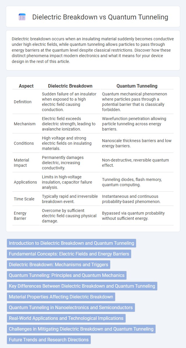
| Aspect | Dielectric Breakdown | Quantum Tunneling |
|---|---|---|
| Definition | Sudden failure of an insulator when exposed to a high electric field causing conduction. | Quantum mechanical phenomenon where particles pass through a potential barrier that is classically forbidden. |
| Mechanism | Electric field exceeds dielectric strength, leading to avalanche ionization. | Wavefunction penetration allowing particle tunneling across energy barriers. |
| Conditions | High voltage and strong electric fields on insulating materials. | Nanoscale thickness barriers and low energy barriers. |
| Material Impact | Permanently damages dielectric, increasing conductivity. | Non-destructive, reversible quantum effect. |
| Applications | Limits in high-voltage insulation, capacitor failure analysis. | Tunneling diodes, flash memory, quantum computing. |
| Time Scale | Typically rapid and irreversible breakdown event. | Instantaneous and continuous probability-based phenomenon. |
| Energy Barrier | Overcome by sufficient electric field causing physical damage. | Bypassed via quantum probability without sufficient energy. |
Introduction to Dielectric Breakdown and Quantum Tunneling
Dielectric breakdown occurs when an insulating material suddenly becomes conductive due to a strong electric field, causing a catastrophic loss of insulation and potential damage in electronic devices. Quantum tunneling is a quantum mechanical phenomenon where particles pass through energy barriers they classically shouldn't overcome, enabling current flow in devices like tunnel diodes and flash memory. Both processes fundamentally influence the behavior and reliability of electronic components at micro and nanoscale dimensions.
Fundamental Concepts: Electric Fields and Energy Barriers
Dielectric breakdown occurs when a strong electric field exceeds the insulating material's dielectric strength, causing a sudden and irreversible flow of current by creating conductive paths through the material. Quantum tunneling involves charged particles penetrating energy barriers with probabilities governed by the barrier width and height, even when classical physics forbids their passage under lower electric fields. These phenomena differ fundamentally as dielectric breakdown relies on macroscopic field-induced damage, while quantum tunneling stems from wavefunction probability amplitudes allowing sub-barrier transmission.
Dielectric Breakdown: Mechanisms and Triggers
Dielectric breakdown occurs when an insulating material experiences a sudden surge of electrical current, caused by an intense electric field that exceeds the material's dielectric strength. This process can be triggered by factors such as material defects, impurities, high temperatures, and prolonged exposure to strong electric fields. The breakdown mechanism involves electron avalanches and the formation of conductive paths, leading to permanent damage or failure of the dielectric material.
Quantum Tunneling: Principles and Quantum Mechanics
Quantum tunneling occurs when particles pass through energy barriers that classical physics deems impenetrable, a phenomenon explained by wavefunction probability in quantum mechanics. The tunneling effect is critical in devices such as tunnel diodes and scanning tunneling microscopes, where electrons effectively "tunnel" through insulating materials. This contrasts with dielectric breakdown, which involves the physical failure of an insulating material due to an intense electric field causing ionization and conduction.
Key Differences Between Dielectric Breakdown and Quantum Tunneling
Dielectric breakdown occurs when an insulating material experiences a critical electric field, causing electrons to abruptly flow and create permanent damage, whereas quantum tunneling involves electrons probabilistically passing through energy barriers without the need for high voltage. Your electronic components rely on dielectric breakdown as a destructive failure mode, while quantum tunneling is a reversible and fundamental quantum phenomenon exploited in devices like tunnel diodes. The key difference lies in dielectric breakdown being a classical, destructive event resulting from macroscopic electric fields, while quantum tunneling is a non-destructive, microscopic effect governed by wave-particle duality and probability.
Material Properties Affecting Dielectric Breakdown
Dielectric breakdown in materials is critically influenced by factors such as dielectric strength, purity, crystalline structure, and temperature, which determine the material's ability to withstand high electric fields without failure. Quantum tunneling, distinct from dielectric breakdown, depends on the electron wavefunction penetration through potential barriers, which is highly sensitive to barrier width and height at the nanoscale. Understanding the interplay between intrinsic material defects and electronic band structure is key to predicting dielectric breakdown thresholds and tunneling probabilities in advanced semiconductors and insulators.
Quantum Tunneling in Nanoelectronics and Semiconductors
Quantum tunneling in nanoelectronics and semiconductors enables electrons to pass through energy barriers at the nanoscale, significantly impacting device performance and scaling. Unlike dielectric breakdown, which involves catastrophic material failure due to high electric fields, quantum tunneling allows controlled electron flow in components such as tunnel diodes and flash memory cells. Understanding this phenomenon is crucial for optimizing your semiconductor devices and advancing nanoscale technology.
Real-World Applications and Technological Implications
Dielectric breakdown is critical in designing high-voltage insulation systems for transformers and capacitors, ensuring device longevity and safety by preventing electrical failure under strong electric fields. Quantum tunneling underpins advancements in semiconductor technology, enabling ultra-fast transistors and novel memory devices like flash storage, where electrons tunnel through energy barriers for data processing. Understanding both phenomena drives innovation in nanoelectronics and energy systems, balancing material limits with quantum effects for optimized performance and miniaturization.
Challenges in Mitigating Dielectric Breakdown and Quantum Tunneling
Mitigating dielectric breakdown involves overcoming material limitations such as impurity-induced defects and high electric fields that accelerate insulation failure, while controlling quantum tunneling challenges requires managing electron wavefunction penetration through ultra-thin barriers in nanoscale devices. Advanced materials engineering aims to enhance dielectric strength and thickness uniformity to reduce breakdown occurrences, and precision nanofabrication targets barrier optimization to suppress tunneling currents without compromising device performance. Understanding electron transport mechanisms at the atomic scale is crucial for developing robust methods to minimize both dielectric breakdown and quantum tunneling in high-performance electronic components.
Future Trends and Research Directions
Future trends in dielectric breakdown research emphasize developing ultra-thin, high-k dielectric materials to enhance device reliability and miniaturization in nanoelectronics. Quantum tunneling studies are advancing toward harnessing tunneling effects for low-power electronic components and quantum computing applications, focusing on material heterostructures and interface engineering. Emerging research integrates machine learning algorithms to predict breakdown thresholds and optimize tunneling phenomena, accelerating innovation in semiconductor technologies.
Dielectric Breakdown vs Quantum Tunneling Infographic