Self-assembled nanowires form through spontaneous chemical or physical processes, offering high precision at the nanoscale but limited control over exact placement and uniformity. Lithographically defined nanowires provide customizable patterns with excellent spatial control, although they often require more complex fabrication techniques and can introduce defects; explore the full article to understand which method best suits your nanotechnology applications.
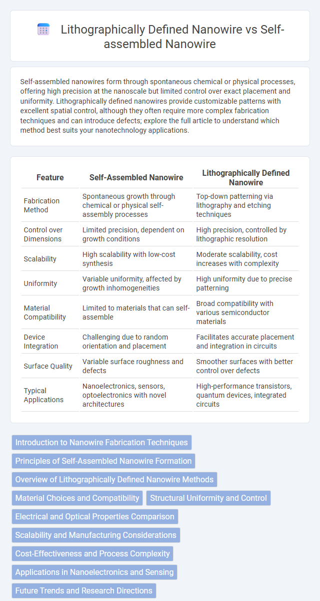
Table of Comparison
| Feature | Self-Assembled Nanowire | Lithographically Defined Nanowire |
|---|---|---|
| Fabrication Method | Spontaneous growth through chemical or physical self-assembly processes | Top-down patterning via lithography and etching techniques |
| Control over Dimensions | Limited precision, dependent on growth conditions | High precision, controlled by lithographic resolution |
| Scalability | High scalability with low-cost synthesis | Moderate scalability, cost increases with complexity |
| Uniformity | Variable uniformity, affected by growth inhomogeneities | High uniformity due to precise patterning |
| Material Compatibility | Limited to materials that can self-assemble | Broad compatibility with various semiconductor materials |
| Device Integration | Challenging due to random orientation and placement | Facilitates accurate placement and integration in circuits |
| Surface Quality | Variable surface roughness and defects | Smoother surfaces with better control over defects |
| Typical Applications | Nanoelectronics, sensors, optoelectronics with novel architectures | High-performance transistors, quantum devices, integrated circuits |
Introduction to Nanowire Fabrication Techniques
Self-assembled nanowires form through bottom-up processes driven by chemical or physical forces, enabling high precision and atomic-scale control ideal for nanoscale electronics and photonics. Lithographically defined nanowires rely on top-down fabrication methods, such as electron beam lithography or photolithography, allowing precise patterning and scalability for integrated circuit applications. Your choice between these techniques depends on the desired structural complexity, device integration, and manufacturing scalability.
Principles of Self-Assembled Nanowire Formation
Self-assembled nanowire formation relies on bottom-up growth mechanisms, where atoms or molecules spontaneously organize into nanowires due to thermodynamic and kinetic factors, such as strain relaxation, surface energy minimization, and catalyst-mediated vapor-liquid-solid (VLS) processes. Unlike lithographically defined nanowires that are patterned top-down with precise dimensions controlled by photolithography or electron-beam lithography, self-assembled nanowires naturally form with uniform crystallinity and strong axial growth along specific crystallographic directions. Understanding these fundamental principles allows your design process to leverage intrinsic material properties for scalable fabrication of high-quality nanowires without complex patterning steps.
Overview of Lithographically Defined Nanowire Methods
Lithographically defined nanowire methods utilize advanced photolithography or electron-beam lithography to create precise, reproducible nanowire patterns on substrates, ensuring consistent dimensions and alignment. These techniques offer high spatial resolution, enabling integration into complex electronic or photonic circuits with tailored properties. Your choice of lithography type significantly influences fabrication accuracy, cost, and scalability in nanowire production.
Material Choices and Compatibility
Self-assembled nanowires often utilize III-V semiconductors like GaAs and InP, offering superior crystal quality and defect reduction, while lithographically defined nanowires primarily rely on silicon and silicon-based materials compatible with standard CMOS processes. The material choices in self-assembled nanowires provide enhanced optoelectronic properties but may face integration challenges with existing fabrication infrastructure. Your project's material compatibility needs will determine whether the high-quality but less standard self-assembled approach or the more industry-compatible lithographic method is the optimal choice.
Structural Uniformity and Control
Self-assembled nanowires exhibit excellent structural uniformity due to their intrinsic growth mechanisms, but they offer limited control over precise positioning and dimensions. Lithographically defined nanowires provide unparalleled control over size, shape, and spatial arrangement, enabling tailored device architectures with nanoscale precision. Your choice depends on whether you prioritize inherent uniformity or customizable nanoscale design for specific applications.
Electrical and Optical Properties Comparison
Self-assembled nanowires exhibit superior electrical conductivity and carrier mobility due to fewer defects and atomically smooth surfaces compared to lithographically defined nanowires, which often suffer from edge roughness and etching-induced damage. Optically, self-assembled nanowires demonstrate enhanced photoluminescence efficiency and wavelength tunability arising from their uniform crystallinity and quantum confinement effects, while lithographically defined nanowires provide better control over dimensions but typically have lower optical quality. The intrinsic material quality in self-assembled structures leads to improved performance in optoelectronic applications such as LEDs and photodetectors compared to their lithographically fabricated counterparts.
Scalability and Manufacturing Considerations
Self-assembled nanowires offer high scalability due to their bottom-up fabrication process, enabling uniform large-area coverage with minimal lithographic intervention, which reduces production costs and complexity. In contrast, lithographically defined nanowires provide precise geometric control but face limitations in scalability caused by the resolution constraints and slower throughput of top-down patterning techniques. Manufacturing considerations favor self-assembled nanowires for mass production in applications like sensors and transistors, while lithographically defined nanowires remain critical for device architectures requiring exact dimensional control and integration.
Cost-Effectiveness and Process Complexity
Self-assembled nanowires offer superior cost-effectiveness by eliminating the need for expensive lithography equipment and complex fabrication steps, reducing material waste and processing time. In contrast, lithographically defined nanowires require intricate patterning techniques such as electron beam lithography, increasing process complexity and production costs. The simplicity of self-assembly enables scalable manufacturing with fewer cleanroom requirements, making it ideal for large-volume applications.
Applications in Nanoelectronics and Sensing
Self-assembled nanowires offer superior atomic-scale precision and defect minimization, enhancing performance in nanoelectronics and sensitive detection applications compared to lithographically defined nanowires, which are limited by patterning resolution and scalability. Your devices benefit from the enhanced electrical conductivity and surface-to-volume ratio of self-assembled nanowires, enabling ultra-sensitive sensors and high-speed transistors. In contrast, lithographically defined nanowires provide better structural uniformity and design flexibility for large-scale integrated circuits but may struggle with nanoscale feature accuracy needed for cutting-edge sensing technologies.
Future Trends and Research Directions
Future trends in self-assembled nanowire research emphasize scalability, defect minimization, and integration with flexible electronics, leveraging bottom-up fabrication for cost-effective nanodevice production. Lithographically defined nanowires continue to advance in precision and complexity, with research focusing on enhancing resolution through novel lithography techniques like EUV and electron-beam lithography to meet the demands of quantum computing and nanoscale sensors. Emerging hybrid approaches combining self-assembly with lithography aim to exploit the strengths of both methods, driving innovations in nanoelectronics and photonics.
Self-assembled Nanowire vs Lithographically Defined Nanowire Infographic