Planar FETs feature a flat, two-dimensional channel, offering simplicity and ease of manufacturing but facing scalability challenges at smaller technology nodes. 3D FETs, such as FinFETs, provide enhanced control over the channel by wrapping the gate around a fin-shaped structure, significantly reducing leakage and improving performance; explore the rest of the article to understand how these differences impact your device's efficiency and power consumption.
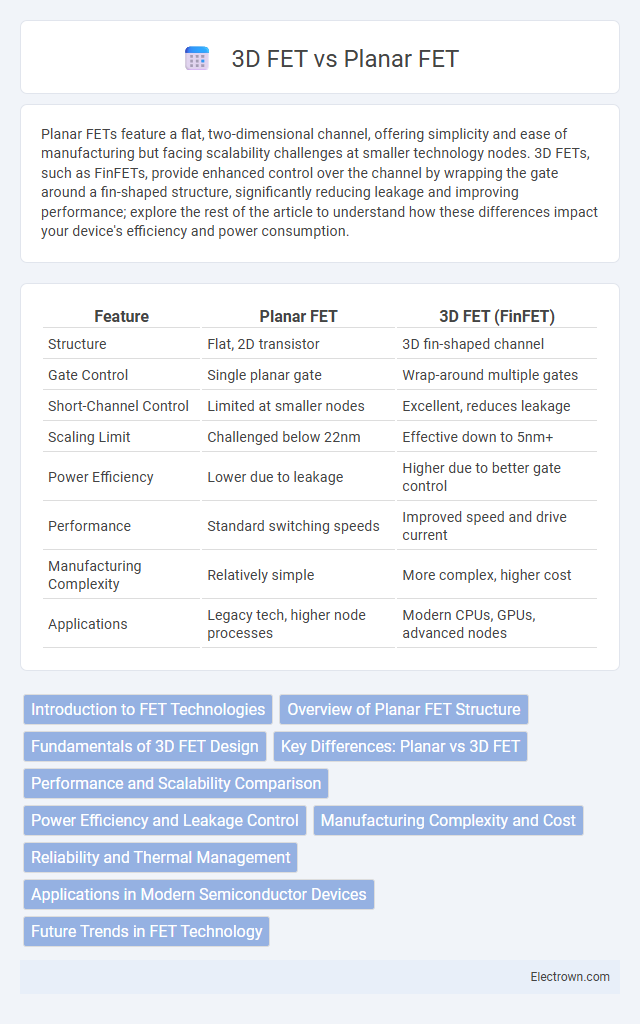
Table of Comparison
| Feature | Planar FET | 3D FET (FinFET) |
|---|---|---|
| Structure | Flat, 2D transistor | 3D fin-shaped channel |
| Gate Control | Single planar gate | Wrap-around multiple gates |
| Short-Channel Control | Limited at smaller nodes | Excellent, reduces leakage |
| Scaling Limit | Challenged below 22nm | Effective down to 5nm+ |
| Power Efficiency | Lower due to leakage | Higher due to better gate control |
| Performance | Standard switching speeds | Improved speed and drive current |
| Manufacturing Complexity | Relatively simple | More complex, higher cost |
| Applications | Legacy tech, higher node processes | Modern CPUs, GPUs, advanced nodes |
Introduction to FET Technologies
Planar FET technology features a flat, two-dimensional structure where the current flows along a single plane, making it simpler but limited in scaling due to short-channel effects. 3D FETs, such as FinFETs, utilize a three-dimensional fin-like structure that enhances gate control over the channel, improving performance and reducing leakage at smaller nodes. Your choice between planar and 3D FETs impacts device efficiency, power consumption, and scalability in advanced semiconductor manufacturing.
Overview of Planar FET Structure
Planar FETs feature a flat, two-dimensional channel structure where the current flows horizontally between the source and drain terminals beneath the gate electrode. This configuration relies on a single silicon surface interface, offering simpler fabrication and reliable electrical characteristics. Your choice of planar FETs suits applications demanding mature technology with well-understood behaviors and cost-effective manufacturing.
Fundamentals of 3D FET Design
3D FET design fundamentally revolves around enhancing channel control by wrapping the gate electrode around the semiconductor channel, significantly reducing short-channel effects compared to planar FETs. The vertical stacking of channels in FinFET or GAAFET architectures increases effective drive current density, improving device scalability and performance at nanometer scales. Optimizing the gate geometry and fin dimensions is critical to achieving high electrostatic integrity and minimizing leakage currents in 3D FETs.
Key Differences: Planar vs 3D FET
Planar FETs utilize a flat, two-dimensional channel where current flows horizontally, while 3D FETs, such as FinFETs, feature a vertical fin-shaped channel enabling multi-gate control to enhance electrostatic control and reduce leakage. The key difference lies in the channel geometry, with 3D FETs offering improved short-channel effects, higher drive current, and better scalability compared to planar FETs. This results in superior performance and power efficiency in advanced semiconductor nodes where 3D FETs dominate over traditional planar structures.
Performance and Scalability Comparison
Planar FETs offer simpler fabrication processes but face significant limitations in performance and scalability due to increased short-channel effects and leakage currents at smaller nodes. 3D FETs, such as FinFETs, provide enhanced electrostatic control, reduced leakage, and improved drive current, enabling better performance and energy efficiency as device dimensions scale down. Your choice of device technology directly impacts the ability to achieve higher transistor densities and maintain operational reliability in advanced semiconductor nodes.
Power Efficiency and Leakage Control
3D FETs offer superior power efficiency and leakage control compared to planar FETs due to their multi-gate architecture, which provides better electrostatic control over the channel. This enhanced control reduces short-channel effects, minimizing leakage currents and lowering overall power consumption. Consequently, 3D FET technology enables higher device density and improved performance for low-power applications relative to traditional planar transistors.
Manufacturing Complexity and Cost
Planar FETs exhibit lower manufacturing complexity due to their simpler 2D structure and established fabrication processes, resulting in reduced production costs. In contrast, 3D FETs, such as FinFETs, require advanced lithography and etching techniques to create multi-gate architectures, significantly increasing manufacturing complexity. The higher fabrication expenses of 3D FETs are offset by improved device performance and scalability in advanced semiconductor nodes.
Reliability and Thermal Management
3D FETs offer superior thermal management compared to Planar FETs due to their vertical channel structure, which enhances heat dissipation and reduces hotspot formation. Planar FETs, while simpler in design, face greater challenges in reliability over prolonged use as heat accumulation can accelerate device degradation and performance loss. The 3D FET architecture improves reliability by maintaining lower operating temperatures and minimizing short-channel effects that often cause failure in planar devices.
Applications in Modern Semiconductor Devices
Planar FETs remain prevalent in low-power and cost-sensitive applications due to their mature fabrication processes and simplicity, while 3D FETs, such as FinFETs, dominate high-performance and advanced semiconductor devices for their superior control over short-channel effects and enhanced drive current. Modern CPUs, GPUs, and mobile processors extensively utilize 3D FET technology to achieve increased transistor density and energy efficiency at sub-7nm nodes. Emerging applications in AI accelerators and 5G transceivers leverage 3D FETs for improved switching speeds and reduced leakage currents, pushing the limits of Moore's Law beyond the capabilities of planar devices.
Future Trends in FET Technology
Future trends in FET technology emphasize the shift from Planar FETs to 3D FETs, such as FinFETs, due to their superior control over channel electrostatics and reduced short-channel effects. 3D FETs enable further device scaling, higher drive currents, and improved energy efficiency, making them critical for next-generation high-performance and low-power applications. Your choice of semiconductor technology will increasingly rely on 3D FET structures to meet the demands of advanced computing and mobile devices.
Planar FET vs 3D FET Infographic