3D NAND technology stacks memory cells vertically to increase storage density and reduce cost per bit, while planar NAND arranges cells in a flat, two-dimensional layout, limiting scaling potential. Discover how these differences impact your device's performance and reliability by reading the full article.
Table of Comparison
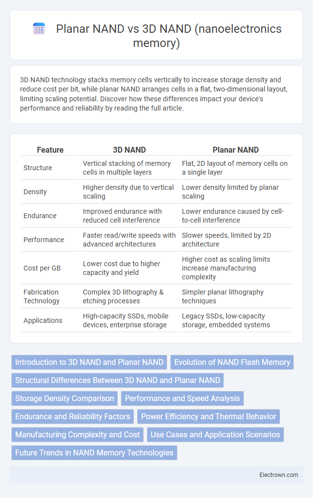
| Feature | 3D NAND | Planar NAND |
|---|---|---|
| Structure | Vertical stacking of memory cells in multiple layers | Flat, 2D layout of memory cells on a single layer |
| Density | Higher density due to vertical scaling | Lower density limited by planar scaling |
| Endurance | Improved endurance with reduced cell interference | Lower endurance caused by cell-to-cell interference |
| Performance | Faster read/write speeds with advanced architectures | Slower speeds, limited by 2D architecture |
| Cost per GB | Lower cost due to higher capacity and yield | Higher cost as scaling limits increase manufacturing complexity |
| Fabrication Technology | Complex 3D lithography & etching processes | Simpler planar lithography techniques |
| Applications | High-capacity SSDs, mobile devices, enterprise storage | Legacy SSDs, low-capacity storage, embedded systems |
Introduction to 3D NAND and Planar NAND
3D NAND memory stacks multiple layers of memory cells vertically, significantly increasing storage density compared to Planar NAND, which arranges cells in a single horizontal layer. Planar NAND uses a two-dimensional cell layout, making it simpler but limited by scaling challenges and increased cell interference. The vertical architecture of 3D NAND enables improved performance, endurance, and capacity, addressing the physical limitations inherent in traditional Planar NAND technology.
Evolution of NAND Flash Memory
3D NAND flash memory represents a significant evolution from planar NAND by stacking memory cells vertically, increasing storage density and reducing cost per bit while enhancing endurance and performance. Planar NAND, limited by two-dimensional scaling and cell-to-cell interference, struggles with smaller process nodes, making 3D NAND's vertical architecture essential for continuing Moore's Law trends. The transition to 3D NAND has enabled the development of high-capacity SSDs and advanced memory solutions critical for mobile, data center, and AI applications.
Structural Differences Between 3D NAND and Planar NAND
3D NAND memory features vertically stacked memory cells, enabling higher density by utilizing the third dimension, unlike Planar NAND which arranges cells in a single horizontal layer. The vertical structure in 3D NAND reduces cell-to-cell interference and short-channel effects common in Planar NAND, improving endurance and reliability. Additionally, 3D NAND's charge trap technology replaces the traditional floating gate used in Planar NAND, enhancing scalability and minimizing electron leakage.
Storage Density Comparison
3D NAND technology significantly increases storage density by stacking multiple memory cells vertically, enabling higher capacity within a smaller footprint compared to planar NAND's two-dimensional layout. This vertical architecture allows 3D NAND to overcome the lithography limitations faced by planar NAND, resulting in more bits per chip and improved scalability. Consequently, 3D NAND offers enhanced storage density, supporting larger SSD capacities and cost-effective memory solutions in nanoelectronics.
Performance and Speed Analysis
3D NAND offers significantly improved performance and speed compared to Planar NAND due to its vertical stacking of memory cells, which reduces latency and increases data transfer rates by enabling more parallelism. The architectural advantage in 3D NAND allows for faster read/write cycles and enhanced endurance, stemming from shorter electron tunneling distances and efficient cell operation. Planar NAND's two-dimensional layout limits scaling and speed, resulting in slower access times and lower throughput relative to the advanced 3D NAND technology.
Endurance and Reliability Factors
3D NAND memory offers significantly improved endurance compared to Planar NAND due to its vertical stacking architecture, which reduces cell-to-cell interference and allows for larger cell sizes that withstand more program/erase cycles. Reliability in 3D NAND is enhanced by advanced error-correction algorithms and better wear-leveling techniques that mitigate data retention issues commonly seen in Planar NAND. Furthermore, 3D NAND demonstrates superior tolerance to program disturb effects and charge leakage, resulting in longer device lifespan and more consistent data integrity under high write-intensive conditions.
Power Efficiency and Thermal Behavior
3D NAND memory demonstrates superior power efficiency compared to Planar NAND by utilizing vertical stacking of memory cells, which reduces the cell-to-cell interference and lowers the overall power consumption during programming and erasing cycles. The thermal behavior of 3D NAND is optimized due to its three-dimensional structure, allowing for better heat dissipation and minimizing thermal-induced degradation, whereas Planar NAND is more prone to heat concentration and associated reliability issues. This enhanced thermal management in 3D NAND results in improved endurance and stability, making it more suitable for high-density memory applications where power efficiency and heat control are critical.
Manufacturing Complexity and Cost
3D NAND involves stacking multiple layers of memory cells vertically, increasing manufacturing complexity due to precise layer alignment and advanced etching techniques, which leads to higher initial production costs compared to planar NAND. Planar NAND, with its single-layer cell structure, benefits from simpler fabrication processes and lower material expenses, resulting in reduced overall manufacturing costs. However, as 3D NAND scales with more layers, economies of scale and enhanced storage density can offset initial costs, making it more cost-effective in large-volume production.
Use Cases and Application Scenarios
3D NAND memory excels in high-capacity storage solutions such as solid-state drives (SSDs) for data centers and consumer electronics due to its vertical stacking architecture that enhances density and endurance. Planar NAND remains suitable for cost-sensitive applications with moderate storage needs, like embedded systems and low-end mobile devices, where simplicity and lower manufacturing costs are prioritized. Enterprise applications favor 3D NAND for its superior performance and reliability in intensive read/write workloads, whereas planar NAND is often utilized in budget-oriented products requiring basic non-volatile memory functions.
Future Trends in NAND Memory Technologies
3D NAND technology is rapidly surpassing Planar NAND by enabling higher storage density and improved endurance through vertically stacked memory cells, addressing planar scaling limitations. Emerging trends emphasize increased layer counts and advanced charge-trap architectures to achieve terabit-level storage capacity while reducing cost per bit. Innovations in materials, such as gate-all-around (GAA) transistors and novel error correction algorithms, further enhance performance and reliability in next-generation NAND memory devices.
3D NAND vs Planar NAND (nanoelectronics memory) Infographic