Short-channel effect refers to the degradation of transistor performance as the channel length decreases, causing threshold voltage reduction and increased leakage current. Drain-induced barrier lowering specifically describes how a high drain voltage lowers the energy barrier at the source-channel junction, further impacting device behavior; explore the article to understand how these phenomena affect your semiconductor devices.
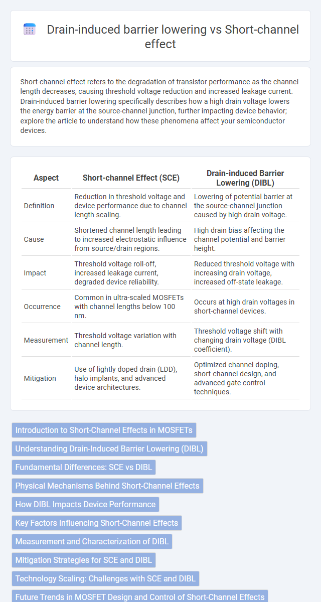
Table of Comparison
| Aspect | Short-channel Effect (SCE) | Drain-induced Barrier Lowering (DIBL) |
|---|---|---|
| Definition | Reduction in threshold voltage and device performance due to channel length scaling. | Lowering of potential barrier at the source-channel junction caused by high drain voltage. |
| Cause | Shortened channel length leading to increased electrostatic influence from source/drain regions. | High drain bias affecting the channel potential and barrier height. |
| Impact | Threshold voltage roll-off, increased leakage current, degraded device reliability. | Reduced threshold voltage with increasing drain voltage, increased off-state leakage. |
| Occurrence | Common in ultra-scaled MOSFETs with channel lengths below 100 nm. | Occurs at high drain voltages in short-channel devices. |
| Measurement | Threshold voltage variation with channel length. | Threshold voltage shift with changing drain voltage (DIBL coefficient). |
| Mitigation | Use of lightly doped drain (LDD), halo implants, and advanced device architectures. | Optimized channel doping, short-channel design, and advanced gate control techniques. |
Introduction to Short-Channel Effects in MOSFETs
Short-channel effects in MOSFETs arise as device channel lengths shrink below the depletion region width, causing threshold voltage variations and degraded device performance. Drain-induced barrier lowering (DIBL) is a primary short-channel effect where high drain voltage lowers the energy barrier for carrier injection, reducing the threshold voltage and increasing leakage current. Understanding these effects is crucial for optimizing transistor scaling in advanced semiconductor technologies.
Understanding Drain-Induced Barrier Lowering (DIBL)
Drain-Induced Barrier Lowering (DIBL) occurs when the electric field from the drain reduces the potential barrier at the source-channel junction, causing increased leakage current and degraded device performance in short-channel MOSFETs. This phenomenon directly impacts your transistor's threshold voltage, leading to reduced gate control and higher off-state current, which complicates device scaling. Understanding DIBL is essential for optimizing semiconductor device design to maintain performance reliability in advanced integrated circuits.
Fundamental Differences: SCE vs DIBL
Short-channel effect (SCE) refers to the overall degradation of transistor performance as channel length decreases, primarily caused by increased electric field coupling between the source and drain, leading to threshold voltage reduction and increased leakage current. Drain-induced barrier lowering (DIBL) is a specific short-channel effect where the drain voltage lowers the potential barrier at the source-channel junction, facilitating easier carrier injection and reducing threshold voltage under high drain bias. The fundamental difference lies in SCE being a broader set of phenomena impacting device scaling, whereas DIBL specifically describes the threshold voltage modulation due to drain bias influence.
Physical Mechanisms Behind Short-Channel Effects
Short-channel effects in MOSFETs arise primarily from the reduced gate control over the channel as the transistor dimensions shrink, leading to phenomena like threshold voltage roll-off and increased leakage currents. Drain-induced barrier lowering (DIBL) occurs when the high drain electric field reduces the potential barrier at the source-channel junction, effectively lowering the threshold voltage and enabling unintended current flow. Understanding these physical mechanisms is crucial for optimizing your device design to minimize performance degradation in nanoscale transistors.
How DIBL Impacts Device Performance
Drain-induced barrier lowering (DIBL) significantly reduces the threshold voltage in short-channel MOSFETs, causing increased off-state leakage current and compromised device reliability. This phenomenon degrades the subthreshold slope and channel control, leading to higher power consumption and reduced switching efficiency. Managing DIBL through optimized channel doping and gate oxide scaling is critical for sustaining device performance in modern nanoscale transistors.
Key Factors Influencing Short-Channel Effects
Key factors influencing short-channel effects include channel length, doping concentration, and oxide thickness, which directly impact the device's electrostatic control and threshold voltage stability. Drain-induced barrier lowering (DIBL) occurs when a high drain voltage reduces the potential barrier, leading to increased off-state current and degraded subthreshold slope. Understanding these factors helps optimize your transistor design for better performance and reduced leakage in advanced nanoscale technologies.
Measurement and Characterization of DIBL
Drain-induced barrier lowering (DIBL) is characterized by measuring the shift in threshold voltage under varying drain bias conditions, typically using I-V and C-V measurements to observe changes in device behavior at different drain voltages. Short-channel effects, including DIBL, are quantified through parameters such as threshold voltage roll-off and subthreshold slope degradation extracted from transfer characteristics. Advanced techniques like pulsed IV measurements and charge pumping can also enhance the accuracy of DIBL characterization in nanoscale MOSFET devices.
Mitigation Strategies for SCE and DIBL
Mitigation strategies for Short-Channel Effect (SCE) include using ultra-thin body devices, high-k gate dielectrics, and advanced channel doping profiles to maintain proper electrostatic control. For Drain-Induced Barrier Lowering (DIBL), increasing channel length, implementing lightly doped drain (LDD) structures, and optimizing gate work function effectively reduce barrier lowering and improve threshold voltage stability. Both effects benefit from multi-gate architectures like FinFETs, which enhance gate control and suppress short-channel phenomena.
Technology Scaling: Challenges with SCE and DIBL
Technology scaling in advanced CMOS devices intensifies short-channel effects (SCE) and drain-induced barrier lowering (DIBL), leading to increased leakage currents and threshold voltage variability. SCE deteriorates device control due to reduced channel length, while DIBL causes a reduction in the energy barrier between the source and channel under high drain bias. Mitigating these effects requires innovations such as high-k gate dielectrics, FinFET architectures, and advanced doping techniques to maintain device performance and reliability at nanometer scales.
Future Trends in MOSFET Design and Control of Short-Channel Effects
Emerging MOSFET designs integrate advanced materials such as high-k dielectrics and novel channel architectures like FinFETs and gate-all-around FETs to mitigate short-channel effects and drain-induced barrier lowering (DIBL). Precision control over channel length scaling and electrostatic integrity is critical for maintaining device performance as transistor dimensions approach the nanometer scale. Your ability to optimize device reliability and threshold voltage stability depends on innovative process techniques and accurate modeling of these short-channel phenomena.
Short-channel effect vs Drain-induced barrier lowering Infographic