GAA FET technology offers superior electrostatic control and reduced short-channel effects compared to traditional FinFETs, enabling enhanced performance and energy efficiency in nanoscale transistors. Explore the rest of the article to understand how Your next-generation semiconductor devices can benefit from GAA FET advancements.
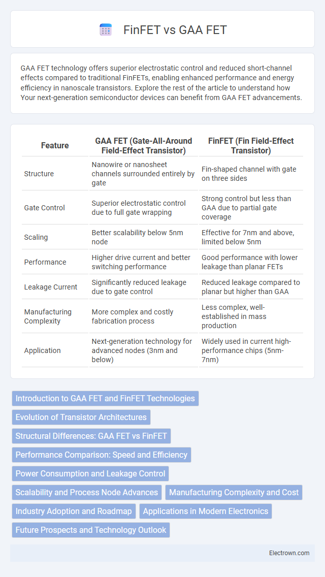
Table of Comparison
| Feature | GAA FET (Gate-All-Around Field-Effect Transistor) | FinFET (Fin Field-Effect Transistor) |
|---|---|---|
| Structure | Nanowire or nanosheet channels surrounded entirely by gate | Fin-shaped channel with gate on three sides |
| Gate Control | Superior electrostatic control due to full gate wrapping | Strong control but less than GAA due to partial gate coverage |
| Scaling | Better scalability below 5nm node | Effective for 7nm and above, limited below 5nm |
| Performance | Higher drive current and better switching performance | Good performance with lower leakage than planar FETs |
| Leakage Current | Significantly reduced leakage due to gate control | Reduced leakage compared to planar but higher than GAA |
| Manufacturing Complexity | More complex and costly fabrication process | Less complex, well-established in mass production |
| Application | Next-generation technology for advanced nodes (3nm and below) | Widely used in current high-performance chips (5nm-7nm) |
Introduction to GAA FET and FinFET Technologies
Gate-All-Around Field-Effect Transistor (GAA FET) and Fin Field-Effect Transistor (FinFET) are advanced semiconductor devices designed to enhance transistor performance and scaling at nanometer technology nodes. FinFET utilizes a 3D fin-shaped channel that improves gate control compared to traditional planar transistors, significantly reducing short-channel effects and leakage currents. GAA FET extends this concept by surrounding the channel completely with the gate, offering superior electrostatic control and enabling further device miniaturization beyond FinFET limitations.
Evolution of Transistor Architectures
GAA (Gate-All-Around) FET represents the latest evolution in transistor architecture, offering superior electrostatic control by surrounding the channel with the gate on all sides, unlike FinFET's three-sided gate structure. This advancement reduces short-channel effects and leakage currents, enabling continued scaling below the 5nm technology node. Your device performance and energy efficiency benefit from GAA FET's enhanced drive current and improved threshold voltage control compared to FinFET technology.
Structural Differences: GAA FET vs FinFET
GAA FET (Gate-All-Around Field-Effect Transistor) features a nanosheet or nanowire channel completely surrounded by the gate, providing improved electrostatic control compared to FinFET's 3D fin-shaped channel partially wrapped by the gate on three sides. This structural difference allows GAA FET to minimize leakage currents and short-channel effects more effectively, enhancing device scalability and performance in advanced semiconductor nodes. Your choice between these architectures impacts power efficiency and transistor density in cutting-edge integrated circuits.
Performance Comparison: Speed and Efficiency
GAA (Gate-All-Around) FETs demonstrate superior electrostatic control compared to FinFETs, resulting in reduced short-channel effects and leakage currents, which significantly enhances overall power efficiency. FinFETs, while offering improved speed over planar transistors, exhibit limitations in scaling below 5nm technology nodes, whereas GAA FETs maintain high drive current and switching speeds at smaller geometries. Performance benchmarks indicate that GAA FETs deliver faster switching speeds and lower power consumption, making them more suitable for advanced, energy-efficient semiconductor devices.
Power Consumption and Leakage Control
GAA FETs offer superior power consumption and leakage control compared to FinFETs due to their enhanced electrostatic control with gate-all-around architecture, which minimizes short-channel effects and reduces off-state leakage currents. The multi-gate structure in GAA FETs enables more effective suppression of leakage, leading to lower static power consumption in advanced technology nodes. Choosing GAA FETs for your design ensures improved energy efficiency and better scalability for low-power applications.
Scalability and Process Node Advances
GAA (Gate-All-Around) FETs offer superior scalability compared to FinFETs by enabling better electrostatic control at sub-5nm process nodes, reducing short-channel effects significantly. Process node advances in GAA devices facilitate higher transistor density and improved performance, supporting the continuation of Moore's Law beyond the limitations encountered by FinFET technology. As a result, GAA FETs represent the forefront of semiconductor development for advanced logic applications in nodes below 3nm.
Manufacturing Complexity and Cost
GAA (Gate-All-Around) FETs present increased manufacturing complexity compared to FinFETs due to their 3D nanowire or nanosheet structures, requiring advanced lithography and precise etching techniques. This complexity results in higher fabrication costs and extended process development time, impacting overall production economics. Your choice between GAA FET and FinFET designs must weigh these manufacturing challenges against performance improvements in next-generation semiconductor devices.
Industry Adoption and Roadmap
GAA (Gate-All-Around) FETs are rapidly gaining traction in the semiconductor industry as the next evolutionary step beyond FinFETs, with companies like Samsung and TSMC targeting mass production around the 3nm node and beyond. FinFET technology dominates current high-volume manufacturing at 7nm and 5nm nodes due to its proven performance and scalability but faces challenges in continued scaling, prompting industry roadmaps to integrate GAA structures for improved electrostatic control and power efficiency. The semiconductor roadmap highlights GAA FETs as the cornerstone for sub-3nm technologies, marking a strategic shift to enable higher transistor densities and lower power consumption in future chips.
Applications in Modern Electronics
Gate-All-Around FETs (GAA FETs) exhibit superior electrostatic control and reduced short-channel effects, making them ideal for advanced logic applications and high-performance computing devices. FinFETs currently dominate mainstream semiconductor manufacturing, powering a wide range of products from smartphones to servers due to their mature fabrication processes and improved speed-efficiency balance. GAA FETs offer enhanced scalability and leakage reduction, positioning them as a promising technology for future nodes in AI accelerators and ultra-low-power IoT devices.
Future Prospects and Technology Outlook
GAA FET technology offers superior electrostatic control and reduced short-channel effects, making it a promising candidate for sub-3nm nodes where FinFET scalability faces limitations. The semiconductor industry's roadmap indicates a transition towards GAA FETs, such as nanosheet and nanowire transistors, to continue device miniaturization and improve power efficiency. Research investments and manufacturing pilots by leading foundries like TSMC and Samsung signal strong future prospects for GAA FETs as the dominant architecture beyond FinFET technology.
GAA FET vs FinFET Infographic