Nanophotonic devices manipulate light at the nanoscale to achieve faster data transmission and lower energy consumption, while nanoelectronic devices focus on controlling electron flow for miniaturized circuits and enhanced processing power. Discover how understanding these differences can optimize Your choice for advanced technology applications in the rest of this article.
Table of Comparison
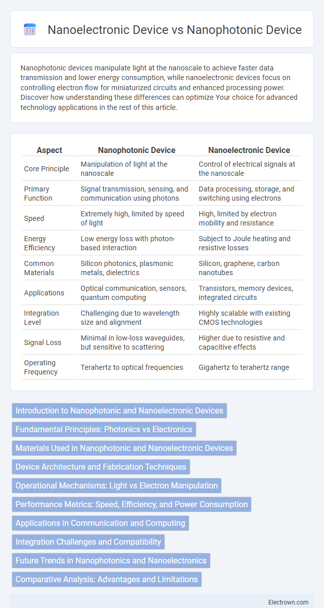
| Aspect | Nanophotonic Device | Nanoelectronic Device |
|---|---|---|
| Core Principle | Manipulation of light at the nanoscale | Control of electrical signals at the nanoscale |
| Primary Function | Signal transmission, sensing, and communication using photons | Data processing, storage, and switching using electrons |
| Speed | Extremely high, limited by speed of light | High, limited by electron mobility and resistance |
| Energy Efficiency | Low energy loss with photon-based interaction | Subject to Joule heating and resistive losses |
| Common Materials | Silicon photonics, plasmonic metals, dielectrics | Silicon, graphene, carbon nanotubes |
| Applications | Optical communication, sensors, quantum computing | Transistors, memory devices, integrated circuits |
| Integration Level | Challenging due to wavelength size and alignment | Highly scalable with existing CMOS technologies |
| Signal Loss | Minimal in low-loss waveguides, but sensitive to scattering | Higher due to resistive and capacitive effects |
| Operating Frequency | Terahertz to optical frequencies | Gigahertz to terahertz range |
Introduction to Nanophotonic and Nanoelectronic Devices
Nanophotonic devices manipulate light at the nanometer scale, leveraging quantum properties to enhance optical communication, sensing, and imaging technologies. Nanoelectronic devices, in contrast, control electrical currents through nanoscale semiconductor components, enabling faster and more energy-efficient transistors and circuits. Your choice between these technologies depends on the desired application in photonics or electronics sectors, balancing speed, power, and integration needs.
Fundamental Principles: Photonics vs Electronics
Nanophotonic devices manipulate light at the nanoscale using principles like electromagnetic wave propagation, photon confinement, and plasmonics to achieve high-speed, low-loss signal transmission. Nanoelectronic devices rely on electron charge transport mechanisms, quantum tunneling, and semiconductor physics to enable miniaturized circuits and enhanced computational power. Photonic devices excel in bandwidth and speed due to photon-based information carriers, whereas electronic devices prioritize charge-based control and integration density.
Materials Used in Nanophotonic and Nanoelectronic Devices
Nanophotonic devices predominantly use materials such as silicon, gallium arsenide, and indium phosphide to manipulate light at the nanoscale, leveraging their optical properties for applications in photonic circuits and sensors. Nanoelectronic devices often rely on silicon, graphene, and transition metal dichalcogenides (TMDs) to enable electron transport and switching at incredibly small dimensions, crucial for high-performance transistors and memory storage. Your choice between these devices hinges on the specific material properties required for either light manipulation or electronic conductivity in your nanoscale technology.
Device Architecture and Fabrication Techniques
Nanophotonic devices utilize nanoscale optical components like waveguides, resonators, and photonic crystals fabricated primarily through lithography, etching, and deposition techniques tailored to manipulate light at subwavelength scales. In contrast, nanoelectronic devices consist of nanoscale transistor elements, quantum dots, and nanowires fabricated using advanced CMOS processes, electron-beam lithography, and molecular self-assembly to control electrical charge transport. Your choice depends on whether device architecture prioritizes photonic signal manipulation or electronic charge control, impacting fabrication methodologies and integration complexity.
Operational Mechanisms: Light vs Electron Manipulation
Nanophotonic devices manipulate light at the nanoscale using principles such as plasmonics and photonic crystals to control photon propagation, confinement, and emission. Nanoelectronic devices rely on electron transport phenomena, quantum tunneling, and charge carrier modulation within nanoscale semiconductor structures to perform electronic functions. While nanophotonics leverages electromagnetic wave behavior for high-speed, low-loss communication, nanoelectronics focuses on electron charge dynamics to achieve miniaturized circuitry and enhanced electrical performance.
Performance Metrics: Speed, Efficiency, and Power Consumption
Nanophotonic devices excel in speed due to light's ultra-fast transmission and minimal signal delay, outperforming nanoelectronic devices in data processing rates. Efficiency in nanophotonic devices is higher as they reduce resistive losses common in nanoelectronics, enabling lower power consumption during high-speed operations. Your system benefits from integrating nanophotonic technology when prioritizing rapid data transfer and energy-efficient performance metrics over traditional nanoelectronic solutions.
Applications in Communication and Computing
Nanophotonic devices leverage light to achieve ultra-fast data transmission and processing, revolutionizing optical communication networks and enabling high-bandwidth, low-latency interconnects in computing systems. Nanoelectronic devices utilize electron-based components at atomic scales to enhance computational speed, energy efficiency, and data storage density, primarily driving advancements in semiconductor technology and miniaturized integrated circuits. Your choice between nanophotonic and nanoelectronic devices can significantly impact the performance and scalability of next-generation communication and computing architectures.
Integration Challenges and Compatibility
Nanophotonic devices face integration challenges due to the need for precise alignment of optical components at the nanoscale, while nanoelectronic devices require compatibility with existing semiconductor fabrication processes. The disparity in operating principles--photons versus electrons--creates material and thermal management complexities when integrating nanophotonic and nanoelectronic components on a single chip. Achieving seamless compatibility demands innovative hybrid materials and novel fabrication techniques to ensure efficient signal transfer and minimize energy loss.
Future Trends in Nanophotonics and Nanoelectronics
Future trends in nanophotonics emphasize the development of ultra-fast optical communication systems and energy-efficient photonic circuits that harness light-matter interactions at the nanoscale. Nanoelectronic devices are advancing towards higher density, lower power consumption, and integration with quantum computing technologies to overcome classical semiconductor limitations. Your ability to leverage these emerging nanotechnologies will shape innovations in computing, sensing, and communication fields.
Comparative Analysis: Advantages and Limitations
Nanophotonic devices offer superior bandwidth and faster data transmission speeds due to the use of photons, enabling low-energy communication and reduced thermal dissipation compared to nanoelectronic devices, which rely on electron flow. Nanoelectronic devices excel in established integration with existing semiconductor technology and demonstrate high-density data storage and processing capabilities; however, they face limitations from resistive heating and electron scattering at nanoscale dimensions. The trade-off between nanophotonics' low latency and low power consumption and nanoelectronics' maturity and miniaturization defines their complementary roles in next-generation computing and communication systems.
Nanophotonic Device vs Nanoelectronic Device Infographic