Quasi-ballistic transport occurs when electrons experience limited scattering, allowing them to maintain partial momentum over short distances, while fully ballistic transport describes electrons moving without any scattering, preserving their energy and momentum through the entire material. Understanding these differences is crucial for optimizing nanoscale device performance, so explore the rest of the article to learn how Your electronic systems can benefit.
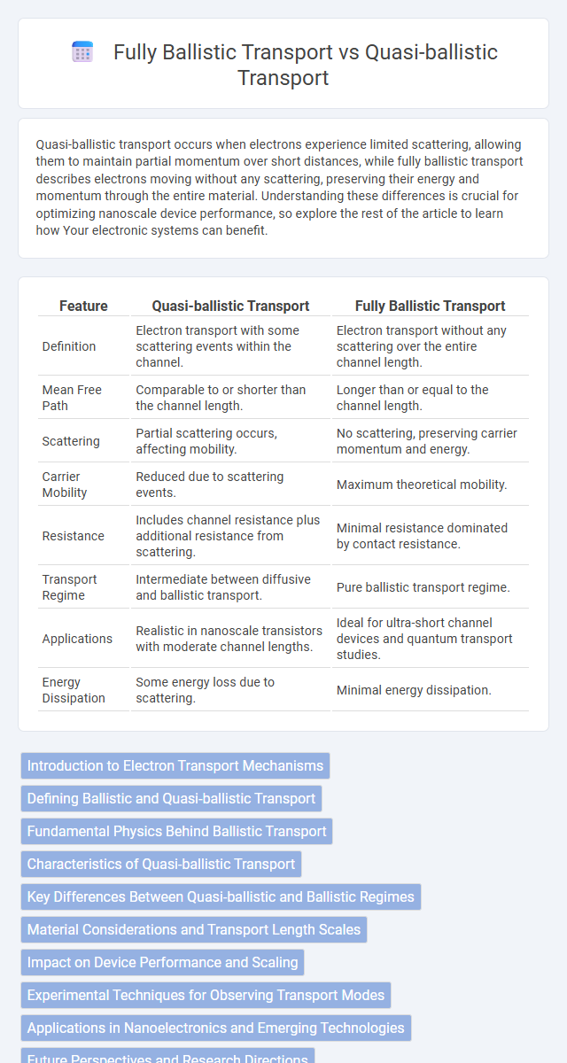
Table of Comparison
| Feature | Quasi-ballistic Transport | Fully Ballistic Transport |
|---|---|---|
| Definition | Electron transport with some scattering events within the channel. | Electron transport without any scattering over the entire channel length. |
| Mean Free Path | Comparable to or shorter than the channel length. | Longer than or equal to the channel length. |
| Scattering | Partial scattering occurs, affecting mobility. | No scattering, preserving carrier momentum and energy. |
| Carrier Mobility | Reduced due to scattering events. | Maximum theoretical mobility. |
| Resistance | Includes channel resistance plus additional resistance from scattering. | Minimal resistance dominated by contact resistance. |
| Transport Regime | Intermediate between diffusive and ballistic transport. | Pure ballistic transport regime. |
| Applications | Realistic in nanoscale transistors with moderate channel lengths. | Ideal for ultra-short channel devices and quantum transport studies. |
| Energy Dissipation | Some energy loss due to scattering. | Minimal energy dissipation. |
Introduction to Electron Transport Mechanisms
Quasi-ballistic transport occurs when electrons travel through a material with some scattering but still retain high mobility, whereas fully ballistic transport features electrons moving without any scattering, maintaining their initial energy and momentum. In nanoscale devices, electron transport mechanisms significantly impact electrical conductivity and device performance, with quasi-ballistic transport allowing partial energy loss but improved current flow compared to diffusive transport. Your understanding of these mechanisms is crucial for optimizing semiconductor devices where controlling electron scattering and mean free paths enhances operational efficiency.
Defining Ballistic and Quasi-ballistic Transport
Ballistic transport refers to the movement of electrons through a material or device without scattering, maintaining their original momentum and energy throughout the channel. Quasi-ballistic transport occurs when electrons experience limited scattering events, resulting in partial momentum preservation and a transport regime between fully ballistic and diffusive conduction. Understanding these regimes is crucial for optimizing nanoscale electronic devices, where channel lengths approach or are shorter than the electron mean free path.
Fundamental Physics Behind Ballistic Transport
Ballistic transport occurs when electrons move through a material without scattering, preserving their momentum and phase coherence, governed by quantum mechanical wavefunctions within nanostructures like quantum wires or carbon nanotubes. In fully ballistic transport, electrons traverse the entire channel length without any collisions, enabling minimal resistance and optimal conductivity as described by Landauer's formula for conductance quantization. Quasi-ballistic transport involves partial scattering events that introduce resistance while maintaining some ballistic characteristics, reflecting the interplay between mean free path and device length in mesoscopic systems.
Characteristics of Quasi-ballistic Transport
Quasi-ballistic transport occurs when charge carriers travel through a material with limited scattering events, maintaining partial coherence over nanometer-scale distances. This transport regime is marked by a mean free path comparable to the device size, resulting in a combination of ballistic and diffusive behaviors. Quasi-ballistic transport influences electronic device performance by reducing resistance and enhancing carrier mobility compared to fully diffusive transport.
Key Differences Between Quasi-ballistic and Ballistic Regimes
Quasi-ballistic transport occurs when charge carriers experience some scattering events within the channel, leading to partial momentum loss, whereas fully ballistic transport involves carriers moving without any scattering, maintaining their momentum throughout. The mean free path in quasi-ballistic regimes is comparable to device dimensions, causing mixed transport characteristics, while in ballistic transport, the mean free path exceeds the device length, resulting in minimal resistance and enhanced carrier velocity. Device performance differences include higher conductance and lower energy dissipation in fully ballistic systems compared to the quasi-ballistic case, where scattering induces resistance and limits electron mobility.
Material Considerations and Transport Length Scales
Quasi-ballistic transport occurs when electrons travel through a material with some scattering events, typically in materials with intermediate mean free paths relative to the device dimensions. Fully ballistic transport happens when electrons move without scattering, requiring materials with long mean free paths and device lengths shorter than these characteristic scattering lengths. Understanding your material's carrier mean free path and ensuring device dimensions align with these transport length scales is crucial for optimizing performance in nanoscale electronic applications.
Impact on Device Performance and Scaling
Quasi-ballistic transport involves partial scattering of charge carriers, leading to moderate performance improvements in nanoscale devices compared to traditional diffusive transport, whereas fully ballistic transport minimizes scattering, maximizing carrier mobility and allowing for ultra-fast switching speeds essential for advanced scaling. Your device performance benefits significantly from fully ballistic transport as it reduces resistance and power dissipation, enabling higher current densities and improved thermal management crucial for continued transistor miniaturization. Understanding the trade-offs between these transport regimes guides engineers in optimizing device design for enhanced scalability and efficiency in next-generation semiconductor technologies.
Experimental Techniques for Observing Transport Modes
Experimental techniques for observing quasi-ballistic transport often involve scanning gate microscopy and low-temperature magnetotransport measurements to detect partial scattering events within nanostructures. Fully ballistic transport is primarily analyzed using quantum point contacts and ballistic electron emission microscopy, which provide clear signatures of scattering-free electron flow. Advanced techniques such as time-resolved terahertz spectroscopy and graphene-based devices enable precise differentiation between quasi-ballistic and fully ballistic regimes by measuring electron mean free paths and coherence lengths.
Applications in Nanoelectronics and Emerging Technologies
Quasi-ballistic transport, characterized by partial scattering of electrons, enables improved performance in nanoscale transistors by balancing speed and thermal management, making it suitable for advanced logic devices and sensors. Fully ballistic transport, where electrons travel without scattering, is crucial for ultra-high-speed nanoelectronic components such as quantum dots, single-electron transistors, and carbon nanotube-based devices, facilitating near-zero energy dissipation. Both transport modes drive innovation in emerging technologies like spintronics, nano-photonics, and flexible electronics by enhancing charge carrier mobility and device scalability at the atomic scale.
Future Perspectives and Research Directions
Future perspectives in quasi-ballistic and fully ballistic transport emphasize enhancing nanoscale device performance by minimizing scattering effects and improving charge carrier mobility. Research directions focus on advanced materials like graphene and topological insulators, along with novel fabrication techniques to achieve near-perfect ballistic conditions at room temperature. Understanding your device's transport regime can guide optimization strategies for next-generation electronics with ultra-high speed and energy efficiency.
Quasi-ballistic Transport vs Fully Ballistic Transport Infographic