Electrostatic doping manipulates charge carrier concentration without altering the material's chemical structure, providing reversible and precise control at the nanoscale, while chemical doping introduces impurities to permanently change electrical properties but can compromise material stability. Explore the rest of the article to understand how these doping methods impact your nanoscale device performance and application choices.
Table of Comparison
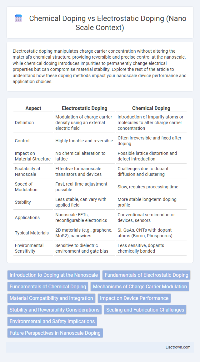
| Aspect | Electrostatic Doping | Chemical Doping |
|---|---|---|
| Definition | Modulation of charge carrier density using an external electric field | Introduction of impurity atoms or molecules to alter charge carrier concentration |
| Control | Highly tunable and reversible | Often irreversible and fixed after doping |
| Impact on Material Structure | No chemical alteration to lattice | Possible lattice distortion and defect introduction |
| Scalability at Nanoscale | Effective for nanoscale transistors and devices | Challenges due to dopant diffusion and clustering |
| Speed of Modulation | Fast, real-time adjustment possible | Slow, requires processing time |
| Stability | Less stable, can vary with applied field | More stable long-term doping profile |
| Applications | Nanoscale FETs, reconfigurable electronics | Conventional semiconductor devices, sensors |
| Typical Materials | 2D materials (e.g., graphene, MoS2), nanowires | Si, GaAs, CNTs with dopant atoms (Boron, Phosphorus) |
| Environmental Sensitivity | Sensitive to dielectric environment and gate bias | Less sensitive, dopants chemically bonded |
Introduction to Doping at the Nanoscale
Doping at the nanoscale involves modifying the electrical properties of nanomaterials by introducing charge carriers through precise methods. Electrostatic doping uses an external electric field to induce charge carriers without altering the material's chemical composition, providing reversible and spatially controlled modulation. Chemical doping incorporates impurity atoms or molecules directly into the nanomaterial, resulting in permanent changes that affect carrier concentration and mobility.
Fundamentals of Electrostatic Doping
Electrostatic doping modulates charge carrier density in nanoscale materials by applying an external electric field through a gate electrode, enabling reversible and precise control without altering the material's chemical composition. This technique relies on the formation of an electric double layer or field effect to induce charge carriers, which enhances device performance and stability compared to chemical doping. Unlike chemical doping, electrostatic doping avoids introducing impurities or defects, preserving the intrinsic properties of nanomaterials such as graphene and transition metal dichalcogenides (TMDs).
Fundamentals of Chemical Doping
Chemical doping at the nanoscale involves introducing impurity atoms or molecules into a semiconductor to modulate its electrical properties by creating charge carriers through ionization. This process relies on the substitutional incorporation or interstitial placement of dopants, which alter the band structure and increase conductivity by providing free electrons or holes. Chemical doping effects are typically permanent and lead to changes in carrier concentration, mobility, and activation energy, critical for tailoring nanoscale device performance.
Mechanisms of Charge Carrier Modulation
Electrostatic doping modulates charge carrier density by applying an external electric field, inducing accumulation or depletion of carriers without altering the material's chemical composition. Chemical doping introduces impurity atoms or molecules, creating fixed charge states that modify carrier concentration through charge transfer or ionization processes. At the nanoscale, electrostatic doping offers reversible and precise control of carrier densities, while chemical doping provides stable but permanent modification of electronic properties.
Material Compatibility and Integration
Electrostatic doping offers superior material compatibility at the nanoscale by enabling reversible charge modulation without introducing impurities or structural defects, making it ideal for sensitive semiconductor materials like graphene and transition metal dichalcogenides. Chemical doping, while effective for permanent carrier concentration adjustment, often involves introducing foreign atoms or molecules that can disrupt the crystal lattice and complicate integration with existing device architectures. Your choice between electrostatic and chemical doping critically impacts the long-term stability and performance of nanoscale electronic devices, especially when seamless integration with diverse materials is required.
Impact on Device Performance
Electrostatic doping offers precise and reversible carrier concentration control at the nanoscale, enabling dynamic tuning of device performance without introducing permanent lattice defects. Chemical doping permanently alters the material's properties by incorporating impurities, which can enhance conductivity but often degrades carrier mobility and increases scattering due to structural disruptions. Your choice between these methods directly affects device stability, speed, and efficiency, with electrostatic doping favoring high-performance, adaptable nano-electronic applications.
Stability and Reversibility Considerations
Electrostatic doping in nanoscale devices offers enhanced reversibility by enabling charge carrier modulation through external electric fields without permanent chemical alterations, ensuring superior device stability during repeated operation cycles. In contrast, chemical doping introduces impurities into the material lattice, which can cause irreversible changes and degrade stability due to dopant diffusion and defect formation over time. The choice between electrostatic and chemical doping strategies significantly impacts the long-term reliability and functional tunability of nanoscale electronic components.
Scaling and Fabrication Challenges
Electrostatic doping enables precise, reversible control of charge carriers at the nanoscale without introducing impurities, making it highly scalable for next-generation devices. Chemical doping involves incorporating foreign atoms, which can cause variability and defects, complicating fabrication and limiting uniformity in ultra-scaled nanoelectronics. Your choice between these methods impacts device performance and manufacturing yield, especially as device dimensions shrink below a few nanometers.
Environmental and Safety Implications
Electrostatic doping at the nanoscale offers a cleaner alternative by avoiding toxic chemicals, reducing environmental contamination risks associated with chemical doping processes. Chemical doping often involves hazardous substances like heavy metals or corrosive agents, posing significant safety challenges for handling, disposal, and worker health. You benefit from electrostatic doping's reversible and non-destructive nature, which minimizes long-term environmental impact and enhances operational safety in nanotechnology applications.
Future Perspectives in Nanoscale Doping
Electrostatic doping offers reversible and precise control over carrier concentration in nanoscale materials, enabling dynamic tuning of electronic properties without altering chemical composition. Chemical doping, while providing stable and permanent modifications, poses challenges in uniformity and scalability at the nanoscale due to dopant diffusion and lattice disruption. Future advancements are expected to combine the stability of chemical doping with the flexibility of electrostatic techniques, leveraging novel materials like two-dimensional semiconductors and advanced gate dielectrics to enhance device performance and enable adaptive nanoscale electronics.
Electrostatic Doping vs Chemical Doping (nano scale context) Infographic