Nanofabrication involves constructing devices and structures at the nanometer scale, enabling precise manipulation of materials for advanced applications like electronics and biotechnology. Understanding the key differences from microfabrication, which operates at the micrometer scale, can help you choose the right techniques for your project; explore the rest of the article to learn more about their distinct processes and applications.
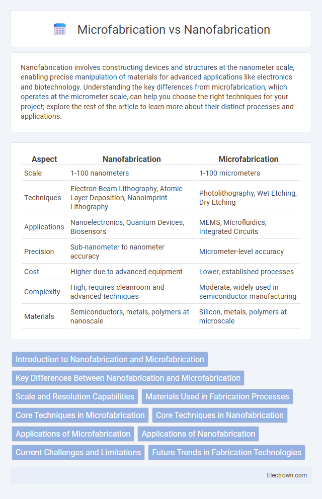
Table of Comparison
| Aspect | Nanofabrication | Microfabrication |
|---|---|---|
| Scale | 1-100 nanometers | 1-100 micrometers |
| Techniques | Electron Beam Lithography, Atomic Layer Deposition, Nanoimprint Lithography | Photolithography, Wet Etching, Dry Etching |
| Applications | Nanoelectronics, Quantum Devices, Biosensors | MEMS, Microfluidics, Integrated Circuits |
| Precision | Sub-nanometer to nanometer accuracy | Micrometer-level accuracy |
| Cost | Higher due to advanced equipment | Lower, established processes |
| Complexity | High, requires cleanroom and advanced techniques | Moderate, widely used in semiconductor manufacturing |
| Materials | Semiconductors, metals, polymers at nanoscale | Silicon, metals, polymers at microscale |
Introduction to Nanofabrication and Microfabrication
Nanofabrication and microfabrication are advanced manufacturing processes for creating structures at nanoscale and microscale levels, respectively. Nanofabrication involves manipulating materials at the atomic or molecular scale, typically below 100 nanometers, enabling innovative applications in electronics, medicine, and materials science. Microfabrication focuses on fabricating features between 1 micrometer and 100 micrometers, commonly used in semiconductor devices, MEMS, and sensors, offering precision critical to your project's performance.
Key Differences Between Nanofabrication and Microfabrication
Nanofabrication involves the manipulation of materials at the nanometer scale (1-100 nm), whereas microfabrication deals with structures sized from 1 to 100 micrometers. Nanofabrication techniques such as electron beam lithography and atomic layer deposition enable the creation of devices with atomic precision, unlike microfabrication processes like photolithography and etching that pattern larger features. The key differences lie in feature size, resolution limits, and the applications ranging from nanoscale electronics and quantum devices to microelectromechanical systems (MEMS) and conventional semiconductor manufacturing.
Scale and Resolution Capabilities
Nanofabrication operates at the nanoscale, typically below 100 nanometers, enabling the creation of structures with atomic or molecular precision, crucial for applications in nanotechnology and advanced electronics. Microfabrication, on the other hand, deals with micrometer-scale features, generally ranging from 1 to 100 micrometers, suitable for producing devices like microelectromechanical systems (MEMS) and integrated circuits. The superior resolution capabilities of nanofabrication allow for densely packed, ultra-small components, while microfabrication offers robust, larger-scale structures optimized for manufacturing efficiency and scalability.
Materials Used in Fabrication Processes
Nanofabrication primarily utilizes advanced materials like silicon, graphene, and carbon nanotubes to create structures at the atomic or molecular scale, enabling unprecedented precision and functionality. Microfabrication commonly employs silicon wafers, photoresists, and metals such as aluminum and gold to build microscale devices essential for semiconductors and MEMS applications. Understanding the distinct materials involved in your fabrication process ensures optimized performance and compatibility with your desired device scale and application.
Core Techniques in Microfabrication
Core techniques in microfabrication include photolithography, etching (both wet and dry), and chemical vapor deposition (CVD), which enable precise patterning and layering at micron scales. Photolithography uses ultraviolet light to transfer geometric patterns onto a substrate coated with a photoresist, essential for defining microstructures. Etching selectively removes material to create microfeatures, while CVD deposits thin films critical for building functional microdevices.
Core Techniques in Nanofabrication
Core techniques in nanofabrication include electron beam lithography, nanoimprint lithography, and atomic layer deposition, which enable precise patterning and layering at the atomic scale. These methods offer superior resolution compared to microfabrication techniques like photolithography, allowing for the creation of structures measured in nanometers rather than micrometers. By leveraging these advanced processes, your ability to develop next-generation nanoelectronic devices and sensors is significantly enhanced.
Applications of Microfabrication
Microfabrication enables the mass production of intricate microscale devices such as MEMS sensors, microfluidic chips, and integrated circuits, playing a vital role in automotive, medical, and consumer electronics industries. This technology facilitates precise control over structural features at the micrometer level, essential for fabricating accelerometers, gyroscopes, inkjet printheads, and lab-on-a-chip systems. The scalability and cost-effectiveness of microfabrication processes drive innovation in telecommunications, biotechnology, and environmental monitoring by providing miniaturized, high-performance components.
Applications of Nanofabrication
Nanofabrication enables the creation of devices and structures at the nanometer scale, driving advancements in electronics, medicine, and energy. Key applications include the development of high-performance transistors, targeted drug delivery systems, and efficient solar cells. Your industry can benefit from enhanced precision and novel materials engineered through nanofabrication techniques.
Current Challenges and Limitations
Nanofabrication faces significant challenges in achieving consistent precision at the atomic scale, including difficulties in controlling material properties and reproducibility. Microfabrication struggles with limitations in feature size reduction, photolithographic resolution, and integration density, impacting device performance and scalability. Your projects may require balancing these constraints to optimize fabrication techniques for specific nanoscale or microscale applications.
Future Trends in Fabrication Technologies
Nanofabrication and microfabrication are advancing towards integration with quantum computing and flexible electronics, emphasizing atomic-level precision and scalability. Emerging trends include the use of advanced materials like 2D nanomaterials and the development of hybrid fabrication processes combining bottom-up and top-down techniques. These innovations drive enhanced device performance, reduced manufacturing costs, and new applications in nanophotonics and bioelectronics.
Nanofabrication vs Microfabrication Infographic