N-type doping introduces extra electrons into nanowires, enhancing their conductivity by increasing negative charge carriers, while P-type doping creates holes by accepting electrons, promoting positive charge carriers for better electrical performance. Explore this article to understand how these doping methods impact your nanowire device applications.
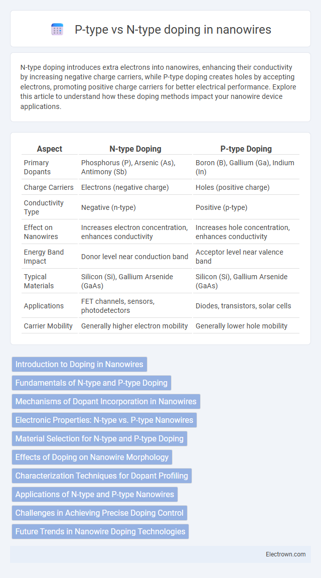
Table of Comparison
| Aspect | N-type Doping | P-type Doping |
|---|---|---|
| Primary Dopants | Phosphorus (P), Arsenic (As), Antimony (Sb) | Boron (B), Gallium (Ga), Indium (In) |
| Charge Carriers | Electrons (negative charge) | Holes (positive charge) |
| Conductivity Type | Negative (n-type) | Positive (p-type) |
| Effect on Nanowires | Increases electron concentration, enhances conductivity | Increases hole concentration, enhances conductivity |
| Energy Band Impact | Donor level near conduction band | Acceptor level near valence band |
| Typical Materials | Silicon (Si), Gallium Arsenide (GaAs) | Silicon (Si), Gallium Arsenide (GaAs) |
| Applications | FET channels, sensors, photodetectors | Diodes, transistors, solar cells |
| Carrier Mobility | Generally higher electron mobility | Generally lower hole mobility |
Introduction to Doping in Nanowires
Doping in nanowires involves introducing impurities to tailor their electrical properties by increasing free charge carriers. N-type doping adds donor atoms, which supply extra electrons, enhancing conductivity, while P-type doping incorporates acceptor atoms that create holes as positive charge carriers. Understanding these mechanisms allows you to precisely control the charge transport behavior essential for nanoscale device applications.
Fundamentals of N-type and P-type Doping
N-type doping in nanowires involves the introduction of donor impurities, such as phosphorus or arsenic, which contribute extra electrons to the conduction band, enhancing electron conductivity. P-type doping incorporates acceptor impurities, like boron or gallium, creating holes by accepting electrons from the valence band, thus increasing hole conductivity. These doping processes fundamentally alter the electrical properties of nanowires by adjusting the carrier concentration and type, enabling tailored semiconductor behavior for nanodevice applications.
Mechanisms of Dopant Incorporation in Nanowires
N-type doping in nanowires typically involves incorporating donor atoms like phosphorus or arsenic, which introduce extra electrons into the conduction band, enhancing electrical conductivity. P-type doping uses acceptor atoms such as boron or gallium that create holes by accepting electrons, facilitating positive charge transport. Your choice of doping method directly affects the mechanisms of dopant incorporation, including solid-source diffusion, vapor-liquid-solid growth, or ion implantation, which influence dopant distribution and activation efficiency within the nanowire structure.
Electronic Properties: N-type vs. P-type Nanowires
N-type doping in nanowires introduces extra electrons, enhancing conductivity by increasing free electron concentration, while P-type doping creates holes that act as positive charge carriers, improving hole mobility. Electronic properties of N-type nanowires typically exhibit higher electron mobility and lower resistivity compared to P-type counterparts, which influence device performance in sensors and transistors. Your choice between N-type and P-type doping directly impacts charge transport characteristics, affecting efficiency and functionality in nanoelectronic applications.
Material Selection for N-type and P-type Doping
Material selection for N-type doping in nanowires typically involves elements with extra valence electrons, such as phosphorus or arsenic in silicon nanowires, to introduce free electrons and enhance conductivity. P-type doping requires materials like boron or gallium that create holes by accepting electrons, effectively increasing positive charge carriers. Your choice of dopants influences the electrical properties and performance of nanowire-based devices, making precise material selection crucial for optimized functionality.
Effects of Doping on Nanowire Morphology
N-type and P-type doping significantly influence nanowire morphology by altering crystal growth dynamics and defect formation. N-type doping typically introduces donors such as phosphorus or arsenic, promoting faster axial growth but possibly increasing surface roughness due to dopant segregation. In contrast, P-type doping with elements like boron often results in reduced growth rates and smoother surfaces, attributed to enhanced surface passivation and altered adatom diffusion.
Characterization Techniques for Dopant Profiling
Characterization techniques for dopant profiling in N-type and P-type doped nanowires include secondary ion mass spectrometry (SIMS) for elemental depth profiling and scanning Kelvin probe microscopy (SKPM) to map surface potential variations related to dopant distribution. Transmission electron microscopy (TEM) combined with electron energy loss spectroscopy (EELS) provides atomic-scale compositional analysis, while capacitance-voltage (C-V) measurements are employed to extract carrier concentration and dopant activation levels. These methods enable precise spatial resolution and quantitative assessment of dopant types and concentrations critical for optimizing nanowire-based electronic devices.
Applications of N-type and P-type Nanowires
N-type nanowires, doped with donor impurities such as phosphorus or arsenic, are widely utilized in high-performance field-effect transistors (FETs) and sensors due to their enhanced electron mobility and conductivity. P-type nanowires, typically doped with acceptor elements like boron, find critical applications in complementary metal-oxide-semiconductor (CMOS) technology and photovoltaic devices where hole transport is essential. Both N-type and P-type nanowires enable the design of nanoscale p-n junctions, which are fundamental in nanoscale diodes, light-emitting devices, and thermoelectric energy conversion systems.
Challenges in Achieving Precise Doping Control
Achieving precise doping control in N-type and P-type nanowires presents significant challenges due to the nanoscale dimensions and surface effects that cause dopant diffusion and clustering, impacting electrical properties. Variability in dopant incorporation often leads to inconsistent carrier concentrations, affecting device performance and scalability. Your ability to optimize doping profiles relies on advanced synthesis techniques and in situ monitoring to mitigate these issues and achieve uniformity.
Future Trends in Nanowire Doping Technologies
Future trends in nanowire doping technologies emphasize precise control over N-type and P-type doping to enhance electronic and optoelectronic device performance. Advanced methods like atomic layer deposition and ion implantation enable tailored carrier concentrations, improving conductivity and enabling applications in nanoscale transistors and sensors. Your ability to leverage these innovations will drive breakthroughs in energy-efficient and high-speed nanoelectronics.
N-type vs P-type doping in nanowires Infographic