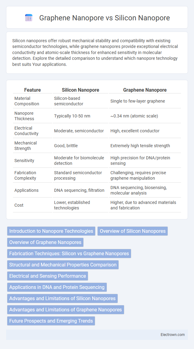
Silicon nanopores offer robust mechanical stability and compatibility with existing semiconductor technologies, while graphene nanopores provide exceptional electrical conductivity and atomic-scale thickness for enhanced sensitivity in molecular detection. Explore the detailed comparison to understand which nanopore technology best suits Your applications.
Table of Comparison
| Feature | Silicon Nanopore | Graphene Nanopore |
|---|---|---|
| Material Composition | Silicon-based semiconductor | Single to few-layer graphene |
| Nanopore Thickness | Typically 10-50 nm | ~0.34 nm (atomic scale) |
| Electrical Conductivity | Moderate, semiconductor | High, excellent conductor |
| Mechanical Strength | Good, brittle | Extremely high tensile strength |
| Sensitivity | Moderate for biomolecule detection | High precision for DNA/protein sensing |
| Fabrication Complexity | Standard semiconductor processing | Challenging, requires precise graphene manipulation |
| Applications | DNA sequencing, filtration | DNA sequencing, biosensing, molecular analysis |
| Cost | Lower, established technologies | Higher, due to advanced materials and fabrication |
Introduction to Nanopore Technologies
Nanopore technologies utilize nanoscale pores to analyze single molecules such as DNA by detecting changes in ionic current as molecules pass through these pores. Silicon nanopores, fabricated through advanced semiconductor processes, offer chemical stability and precise size control, making them suitable for integrated electronic biosensors. Graphene nanopores, characterized by their atomically thin structure, provide exceptional sensitivity and high spatial resolution due to minimal membrane thickness and excellent electrical conductivity.
Overview of Silicon Nanopores
Silicon nanopores are nanoscale holes fabricated in silicon substrates, widely used for biomolecule sensing and DNA sequencing due to their mechanical stability and compatibility with semiconductor technology. These nanopores offer high precision in size control during fabrication processes such as focused ion beam milling and electron beam lithography, enabling selective molecular analysis. Compared to graphene nanopores, silicon nanopores exhibit better integration with electronic circuits but generally feature thicker membranes, which can affect resolution in single-molecule detection.
Overview of Graphene Nanopores
Graphene nanopores are ultra-thin membranes consisting of a single layer of carbon atoms arranged in a hexagonal lattice, enabling high electrical conductivity and mechanical strength. This atomic-scale thickness allows for precise DNA sequencing and molecular sensing with enhanced sensitivity compared to silicon nanopores, which are typically thicker and less conductive. Your choice of nanopore technology can significantly impact the resolution and accuracy of biomolecular detection due to graphene's superior chemical stability and tunable pore size.
Fabrication Techniques: Silicon vs Graphene Nanopores
Silicon nanopores are fabricated using well-established semiconductor processes like photolithography, reactive ion etching, and focused ion beam milling, enabling precise control over pore size and geometry. In contrast, graphene nanopores are created through electron beam sculpting or controlled dielectric breakdown, leveraging graphene's atomic thickness for ultra-sensitive molecular detection. Your choice between silicon and graphene nanopores hinges on fabrication complexity, resolution, and application specificity.
Structural and Mechanical Properties Comparison
Silicon nanopores exhibit high mechanical stability and compatibility with standard semiconductor fabrication, characterized by a rigid crystalline lattice and robust thermal resilience. Graphene nanopores offer exceptional tensile strength and atomic-scale thickness, enabling superior sensitivity and minimal noise in molecular sensing applications. The ultrathin graphene membranes provide enhanced spatial resolution, whereas silicon nanopores afford greater structural durability under high-pressure or high-temperature conditions.
Electrical and Sensing Performance
Silicon nanopores exhibit robust electrical stability with low noise levels, enabling precise ionic current measurements crucial for high-fidelity sensing applications. Graphene nanopores offer exceptional electrical conductivity and atomic thickness, resulting in enhanced signal-to-noise ratio and superior spatial resolution for biomolecule detection. Both materials show distinct advantages in electrical and sensing performance, where silicon's durability contrasts with graphene's ultra-sensitive single-molecule analysis capabilities.
Applications in DNA and Protein Sequencing
Silicon nanopores offer precise control and compatibility with established semiconductor technology, making them ideal for high-throughput DNA sequencing applications that require robust signal modulation. Graphene nanopores provide exceptional sensitivity due to their atomic thickness, enabling enhanced resolution in protein sequencing by detecting subtle biomolecular interactions. Your choice depends on whether you prioritize scalability and integration (silicon) or ultra-high sensitivity and single-molecule detection capabilities (graphene).
Advantages and Limitations of Silicon Nanopores
Silicon nanopores offer precise and tunable pore sizes, enabling high-resolution molecular sensing essential for DNA sequencing and biomolecule analysis. Their compatibility with established semiconductor fabrication techniques enhances integration with electronic devices, although silicon's brittleness and susceptibility to surface charge variability can limit device robustness and consistency. You may find that while silicon nanopores provide excellent control and scalability, challenges remain in achieving long-term stability compared to more chemically inert alternatives like graphene nanopores.
Advantages and Limitations of Graphene Nanopores
Graphene nanopores offer exceptional electrical conductivity and atomic thinness, enabling high-resolution single-molecule detection and improved sensitivity compared to silicon nanopores. Their mechanical strength and chemical stability make them suitable for diverse sensing environments, but challenges such as pore size control and susceptibility to contamination limit reproducibility and scalability. Despite these limitations, graphene nanopores' unique electronic properties provide promising potential for advanced biosensing applications.
Future Prospects and Emerging Trends
Silicon nanopores demonstrate strong potential for scalable integration in semiconductor devices due to their compatibility with existing silicon-based technologies, enabling advanced sensing applications in genomics and proteomics. Graphene nanopores offer exceptional electrical sensitivity and atomic thickness, making them ideal for single-molecule detection and rapid DNA sequencing, which drives innovation in personalized medicine. Emerging trends emphasize hybrid nanopore systems combining silicon's mechanical robustness with graphene's electrical properties to optimize performance for next-generation biosensors and nanoelectronic devices.
Silicon Nanopore vs Graphene Nanopore Infographic