Silicon nanowire FETs offer excellent compatibility with existing semiconductor fabrication processes and provide superior electrostatic control, while carbon nanotube FETs boast exceptional electron mobility and potential for miniaturization beyond silicon limits. Explore this article to understand how your choice between these technologies can impact device performance and future applications.
Table of Comparison
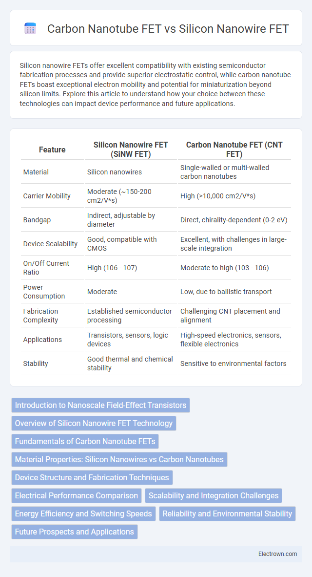
| Feature | Silicon Nanowire FET (SiNW FET) | Carbon Nanotube FET (CNT FET) |
|---|---|---|
| Material | Silicon nanowires | Single-walled or multi-walled carbon nanotubes |
| Carrier Mobility | Moderate (~150-200 cm2/V*s) | High (>10,000 cm2/V*s) |
| Bandgap | Indirect, adjustable by diameter | Direct, chirality-dependent (0-2 eV) |
| Device Scalability | Good, compatible with CMOS | Excellent, with challenges in large-scale integration |
| On/Off Current Ratio | High (106 - 107) | Moderate to high (103 - 106) |
| Power Consumption | Moderate | Low, due to ballistic transport |
| Fabrication Complexity | Established semiconductor processing | Challenging CNT placement and alignment |
| Applications | Transistors, sensors, logic devices | High-speed electronics, sensors, flexible electronics |
| Stability | Good thermal and chemical stability | Sensitive to environmental factors |
Introduction to Nanoscale Field-Effect Transistors
Nanoscale field-effect transistors (FETs) based on silicon nanowires and carbon nanotubes offer unique advantages for next-generation electronics. Silicon nanowire FETs provide compatibility with existing semiconductor fabrication processes, enabling high integration density and scalability in electronic circuits. Carbon nanotube FETs, leveraging exceptional carrier mobility and ballistic transport properties, offer enhanced performance in speed and energy efficiency for your nanoscale device applications.
Overview of Silicon Nanowire FET Technology
Silicon nanowire field-effect transistors (SiNW FETs) utilize ultra-thin silicon wires as the channel material, offering excellent electrostatic control and scalability for next-generation nanoelectronics. These devices boast compatibility with existing silicon technology, enabling seamless integration into current semiconductor manufacturing processes while delivering high electron mobility and low power consumption. Your applications benefit from the SiNW FET's sensitivity and tunable electrical properties, making it ideal for sensors and low-power digital circuits compared to carbon nanotube FETs.
Fundamentals of Carbon Nanotube FETs
Carbon Nanotube Field-Effect Transistors (CNTFETs) utilize carbon nanotubes as the channel material, offering superior electron mobility and ballistic transport compared to silicon nanowires. The unique one-dimensional structure of carbon nanotubes enables near-ideal gate control and reduced short-channel effects, enhancing device performance and energy efficiency. Intrinsic properties such as high current density, chemical stability, and tunable bandgap make CNTFETs promising for next-generation nanoelectronics beyond conventional silicon-based FETs.
Material Properties: Silicon Nanowires vs Carbon Nanotubes
Silicon nanowires exhibit excellent compatibility with existing semiconductor processes, offering reliable electrical properties and well-understood doping techniques crucial for field-effect transistor (FET) applications. Carbon nanotubes provide superior electron mobility and ballistic transport characteristics, enabling higher current densities and faster switching speeds in FET devices. Your choice between these materials impacts device performance, scalability, and integration complexity due to their distinct structural and electronic properties.
Device Structure and Fabrication Techniques
Silicon nanowire FETs utilize a single-crystalline silicon nanowire as the channel, often fabricated through top-down lithography or bottom-up vapor-liquid-solid growth, allowing for precise control over dimensions and doping profiles. Carbon nanotube FETs employ semiconducting carbon nanotubes as the channel material, typically synthesized via chemical vapor deposition and incorporated using transfer printing or direct growth on substrates, which introduces challenges in alignment and purity. Your choice between these devices hinges on the fabrication complexity and the desired device uniformity, with silicon nanowires favoring mature CMOS-compatible processes and carbon nanotubes offering superior electrical properties but requiring advanced assembly techniques.
Electrical Performance Comparison
Silicon nanowire FETs exhibit high current drive capability and mature fabrication processes, leading to reliable electrical performance with good scalability. Carbon nanotube FETs offer superior carrier mobility and near-ballistic transport, resulting in higher ON-state current and faster switching speeds. Despite challenges in uniformity and integration, CNT-FETs demonstrate lower subthreshold swing and enhanced electrostatic control compared to SiNW-FETs, promising improved energy efficiency and device performance.
Scalability and Integration Challenges
Silicon nanowire FETs offer better scalability due to compatibility with existing CMOS fabrication processes, enabling easier integration into current semiconductor manufacturing lines. Carbon nanotube FETs face challenges in uniform alignment, precise placement, and variability control, which complicate large-scale integration and reproducibility. Your choice between these technologies should consider silicon nanowires' mature process compatibility versus carbon nanotubes' potential for higher mobility but greater integration hurdles.
Energy Efficiency and Switching Speeds
Silicon nanowire FETs offer moderate energy efficiency and reliable switching speeds due to their well-established fabrication processes and mature technology. Carbon nanotube FETs excel in energy efficiency with lower power consumption and faster switching speeds attributed to their exceptional electrical conductivity and high carrier mobility. Your choice between these technologies depends on the specific application requirements, prioritizing either the integration maturity of silicon nanowires or the superior performance potential of carbon nanotubes.
Reliability and Environmental Stability
Silicon nanowire FETs exhibit higher reliability in conventional semiconductor environments due to their well-established fabrication processes and inherent material stability. Carbon nanotube FETs, while offering exceptional electrical properties, face challenges in environmental stability caused by sensitivity to moisture, oxygen, and substrate interactions. Enhancing the encapsulation and passivation techniques can improve the durability of your carbon nanotube FET devices for practical applications.
Future Prospects and Applications
Silicon nanowire FETs offer compatibility with existing semiconductor fabrication processes, making them highly scalable for future integrated circuits and advanced sensing applications. Carbon nanotube FETs excel in high electron mobility and flexibility, promising breakthroughs in flexible electronics, high-performance computing, and nano-scale sensors. Your choice between these technologies depends on specific application requirements, where silicon nanowires suit mass production and carbon nanotubes drive cutting-edge, high-speed device innovations.
Silicon nanowire FET vs Carbon nanotube FET Infographic