Split-gate FETs provide enhanced control over the channel by using two separate gate sections, improving noise performance and enabling advanced memory applications compared to common-gate FETs, which are often used for impedance matching and low input capacitance in RF circuits. Explore the rest of the article to understand how these differences impact your device design and performance considerations.
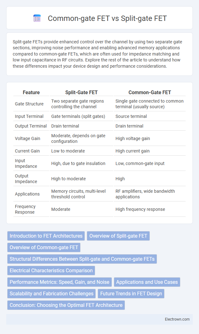
Table of Comparison
| Feature | Split-Gate FET | Common-Gate FET |
|---|---|---|
| Gate Structure | Two separate gate regions controlling the channel | Single gate connected to common terminal (usually source) |
| Input Terminal | Gate terminals (split gates) | Source terminal |
| Output Terminal | Drain terminal | Drain terminal |
| Voltage Gain | Moderate, depends on gate configuration | High voltage gain |
| Current Gain | Low to moderate | High current gain |
| Input Impedance | High, due to gate insulation | Low, common-gate input |
| Output Impedance | High to moderate | High |
| Applications | Memory circuits, multi-level threshold control | RF amplifiers, wide bandwidth applications |
| Frequency Response | Moderate | High frequency response |
Introduction to FET Architectures
Split-gate FET features two separate gates controlling the channel, enabling enhanced electrostatic control and reduced short-channel effects compared to common-gate FET, where a single gate terminal controls the channel with the source grounded. This architecture difference impacts device parameters such as threshold voltage stability, transconductance, and leakage current, with split-gate FET offering superior scalability for advanced CMOS technologies. Common-gate FETs are typically used in high-frequency analog applications due to their low input impedance and better isolation between gate and source terminals.
Overview of Split-gate FET
Split-gate FETs feature two distinct gate electrodes that enable enhanced control over the channel, reducing leakage currents and improving switching speed compared to common-gate FETs. Their architecture allows for better suppression of short-channel effects, making them ideal for high-performance and low-power applications. You can leverage split-gate FET designs to achieve improved device scalability and reliability in advanced semiconductor technologies.
Overview of Common-gate FET
Common-gate FETs feature the gate terminal connected to a constant voltage, serving as a reference for input signal variations at the source terminal, making them ideal for high-frequency applications due to reduced Miller capacitance effects. This configuration offers low input impedance and high output impedance, beneficial for wideband amplifiers and impedance matching. Understanding these characteristics helps you select the appropriate transistor configuration for optimized circuit performance in RF and analog signal processing.
Structural Differences Between Split-gate and Common-gate FETs
Split-gate FETs feature two separate gate electrodes placed along the channel, enabling independent control of different channel regions to enhance device performance and reduce short-channel effects. Common-gate FETs have a single gate terminal connected to a reference node, with the input signal applied to the source terminal while the drain serves as the output, providing low input impedance and high-frequency operation. Structurally, the split-gate design introduces a dual-gate configuration enabling voltage distribution control, whereas the common-gate structure maintains a single gate that directly modulates the channel conductivity from one side.
Electrical Characteristics Comparison
Split-gate FET exhibits enhanced gate control that significantly reduces short-channel effects and improves subthreshold slope compared to common-gate FET, leading to lower off-state leakage currents. Common-gate FETs, characterized by a fixed gate electrode potential, typically demonstrate higher gain and better input-output isolation but suffer from increased gate-to-drain capacitance and reduced voltage gain. Electrical performance in split-gate FETs is optimized for low-power applications with superior threshold voltage stability, while common-gate FETs are favored in high-frequency amplification due to their intrinsic low input impedance and better noise immunity.
Performance Metrics: Speed, Gain, and Noise
Split-gate FETs offer enhanced speed and gain compared to common-gate FETs due to improved channel control and reduced short-channel effects. Your circuits benefit from lower noise levels in split-gate configurations, making them ideal for high-frequency applications requiring superior signal integrity. Common-gate FETs, while stable and providing good input-output isolation, typically exhibit higher noise figures and lower gain, limiting their performance in ultra-fast amplification tasks.
Applications and Use Cases
Split-gate FETs are primarily used in non-volatile memory devices such as flash memory, offering precise charge control for data storage applications. Common-gate FETs find widespread use in high-frequency amplifiers and RF circuits, providing excellent input impedance matching and stability in radio communication systems. Both transistor types serve specialized roles, with split-gate FETs optimized for data retention and common-gate FETs excelling in signal amplification and impedance control.
Scalability and Fabrication Challenges
Split-gate FETs offer enhanced scalability due to their precise gate control, enabling continued device miniaturization while maintaining performance. Their fabrication requires advanced lithography and etching techniques, increasing process complexity and cost compared to common-gate FETs. You must weigh these challenges against the simpler, more mature fabrication processes of common-gate FETs, which may limit scalability but offer easier integration in conventional manufacturing.
Future Trends in FET Design
Split-gate FETs are gaining attention for their ability to reduce short-channel effects and improve control over the channel, making them highly suitable for future nanoscale transistor designs. Common-gate FETs, while offering high-frequency performance and low input impedance, face limitations in scalability as device dimensions shrink. Your choice between these structures will increasingly depend on the balance between high-speed operation and device miniaturization in next-generation semiconductor technologies.
Conclusion: Choosing the Optimal FET Architecture
Split-gate FETs offer enhanced control over channel conduction with reduced short-channel effects, making them ideal for high-performance and low-power applications. Common-gate FETs provide superior high-frequency response and low input impedance, suited for RF and analog amplification circuits. Selecting the optimal FET architecture depends on balancing trade-offs between control precision, frequency performance, and specific application requirements.
Split-gate FET vs Common-gate FET Infographic