SPM (Scanning Probe Microscopy) offers high-resolution surface imaging by scanning a physical probe over the specimen, enabling analysis of surface topography at the atomic scale without requiring conductive samples, unlike SEM (Scanning Electron Microscopy), which uses electron beams to produce detailed images but often requires sample coating and vacuum conditions. Discover how understanding the differences between SPM and SEM can enhance your selection of the optimal microscopy technique by reading the full article.
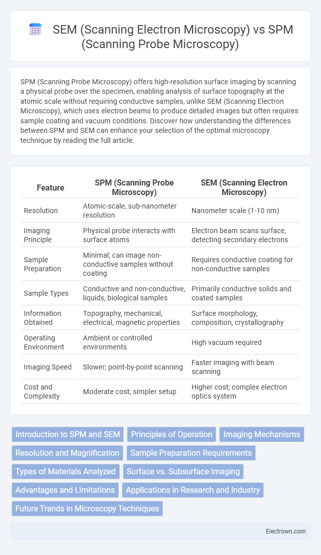
Table of Comparison
| Feature | SPM (Scanning Probe Microscopy) | SEM (Scanning Electron Microscopy) |
|---|---|---|
| Resolution | Atomic-scale, sub-nanometer resolution | Nanometer scale (1-10 nm) |
| Imaging Principle | Physical probe interacts with surface atoms | Electron beam scans surface, detecting secondary electrons |
| Sample Preparation | Minimal; can image non-conductive samples without coating | Requires conductive coating for non-conductive samples |
| Sample Types | Conductive and non-conductive, liquids, biological samples | Primarily conductive solids and coated samples |
| Information Obtained | Topography, mechanical, electrical, magnetic properties | Surface morphology, composition, crystallography |
| Operating Environment | Ambient or controlled environments | High vacuum required |
| Imaging Speed | Slower; point-by-point scanning | Faster imaging with beam scanning |
| Cost and Complexity | Moderate cost; simpler setup | Higher cost; complex electron optics system |
Introduction to SPM and SEM
SPM (Scanning Probe Microscopy) employs a physical probe to scan surfaces at the atomic level, enabling high-resolution imaging and measurement of surface properties such as topography, friction, and magnetic forces. SEM (Scanning Electron Microscopy) uses a focused electron beam to generate detailed images by scanning a sample's surface, providing information about morphology and composition with nanometer-scale resolution. Both techniques are essential for material characterization but differ in imaging mechanisms and sample preparation requirements.
Principles of Operation
SPM (Scanning Probe Microscopy) operates by physically scanning a sharp probe over a sample surface to measure forces or interactions at the atomic or molecular scale, enabling high-resolution topographical mapping. SEM (Scanning Electron Microscopy) uses a focused beam of electrons to scan the sample, detecting secondary or backscattered electrons to generate detailed images based on surface morphology and composition. Your choice depends on whether you prioritize atomic-level surface forces (SPM) or high-resolution imaging with elemental contrast (SEM).
Imaging Mechanisms
SPM (Scanning Probe Microscopy) uses a physical probe that scans the surface to measure interactions such as atomic forces, enabling nanoscale topographical imaging without requiring conductive samples. SEM (Scanning Electron Microscopy) relies on an electron beam that interacts with the sample's surface to generate secondary electrons, producing high-resolution images primarily dependent on the material's electron density and conductivity. Your choice between SPM and SEM should consider the sample's nature and the desired resolution based on these fundamentally different imaging mechanisms.
Resolution and Magnification
SPM (Scanning Probe Microscopy) achieves atomic-scale resolution by physically scanning a sharp probe over the sample surface, surpassing SEM's resolution limits which are typically around 1 nanometer. SEM (Scanning Electron Microscopy) offers higher magnification capabilities, ranging from 10x to over 1,000,000x, enabling detailed imaging of surface topography with excellent depth of field. Your choice between SPM and SEM depends on whether ultra-high resolution for nanoscale surface features or extensive magnification for broader structural analysis is more critical to your application.
Sample Preparation Requirements
SPM (Scanning Probe Microscopy) requires minimal sample preparation, often allowing direct imaging of samples in ambient or liquid environments without conductive coatings. SEM (Scanning Electron Microscopy) typically necessitates extensive preparation, including dehydration, fixation, and conductive coating for insulating materials to prevent charging effects. Your choice between SPM and SEM will depend on the sample's nature and the required resolution, as SPM offers surface topography at the nanoscale with less prep, while SEM delivers high-resolution imaging but with more complex sample preparation.
Types of Materials Analyzed
SPM (Scanning Probe Microscopy) excels in analyzing a wide range of materials, including non-conductive, biological, and soft samples, due to its ability to operate in ambient or liquid environments without the need for conductive coatings. SEM (Scanning Electron Microscopy) primarily targets conductive or metal-coated samples, commonly used for metals, semiconductors, and hard materials, offering high-resolution surface imaging but requiring vacuum conditions. The complementary nature of SPM and SEM enables comprehensive analysis across diverse material types, spanning from polymers and biomolecules to alloys and ceramics.
Surface vs. Subsurface Imaging
SPM (Scanning Probe Microscopy) excels at surface imaging by providing atomic-level topographical details through physical probe interactions, making it ideal for analyzing surface texture, roughness, and nanoscale features. SEM (Scanning Electron Microscopy) enables subsurface imaging by detecting secondary electrons and backscattered electrons, revealing compositional contrasts and subsurface structures beneath the sample's surface. The complementary use of SPM and SEM allows comprehensive characterization, combining precise surface morphology with internal material composition insights.
Advantages and Limitations
SPM offers nanoscale surface characterization with atomic resolution and the ability to analyze non-conductive samples without extensive preparation, making it ideal for delicate materials. SEM provides high-resolution imaging over larger areas with faster acquisition times and detailed compositional analysis through EDS but requires conductive samples or coating, limiting its use on some specimens. Your choice depends on the need for atomic-scale precision and surface interaction (SPM) versus broader imaging and elemental data (SEM).
Applications in Research and Industry
SPM (Scanning Probe Microscopy) excels in nanoscale surface characterization, enabling atomic-level imaging and manipulation critical for materials science, semiconductor development, and molecular biology research. SEM (Scanning Electron Microscopy) offers high-resolution imaging over larger areas, ideal for analyzing surface topography, composition, and microstructures in metallurgy, failure analysis, and quality control in manufacturing. Both techniques complement each other by providing detailed surface morphology insights across different scales and sample types, driving innovation in nanotechnology and industrial process optimization.
Future Trends in Microscopy Techniques
Future trends in microscopy techniques emphasize the convergence of SPM (Scanning Probe Microscopy) and SEM (Scanning Electron Microscopy) to achieve higher resolution and multifunctional imaging capabilities. Advances in hybrid systems and AI-driven image analysis are enhancing the depth of surface characterization and real-time data interpretation. Your research can benefit significantly from these emerging technologies, which promise unprecedented nanoscale insight and automation.
SPM (Scanning Probe Microscopy) vs SEM (Scanning Electron Microscopy) Infographic