Bandgap engineering manipulates the energy difference between the valence and conduction bands to tailor semiconductor properties for specific electronic and optoelectronic applications. Understanding how strain engineering alters the crystal lattice to modify band structure and carrier mobility can further enhance your device performance; explore the full article to discover the benefits and applications of each technique.
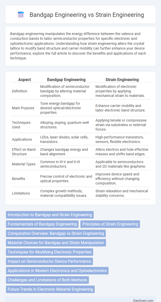
Table of Comparison
| Aspect | Bandgap Engineering | Strain Engineering |
|---|---|---|
| Definition | Modification of semiconductor bandgap by altering material composition. | Modification of electronic properties by applying mechanical strain to materials. |
| Main Purpose | Tune energy bandgap for desired optical/electronic properties. | Enhance carrier mobility and tailor electronic band structure. |
| Techniques Used | Alloying, doping, quantum well structures. | Applying tensile or compressive strain via substrates or external forces. |
| Applications | LEDs, laser diodes, solar cells, transistors. | High-performance transistors, sensors, flexible electronics. |
| Effect on Band Structure | Changes bandgap energy and band alignment. | Alters electron and hole effective masses and shifts band edges. |
| Material Types | Common in III-V and II-VI semiconductors. | Applicable to semiconductors and 2D materials like graphene. |
| Benefits | Precise control of electronic and optical properties. | Improves device speed and efficiency without changing composition. |
| Limitations | Complex growth methods; material compatibility issues. | Strain relaxation and mechanical stability concerns. |
Introduction to Bandgap and Strain Engineering
Bandgap engineering involves modifying the energy difference between the valence band and conduction band in semiconductors to optimize electronic and optical properties. Strain engineering applies mechanical deformation to alter the crystal lattice, enhancing carrier mobility and modifying band structures. Both techniques play critical roles in designing high-performance electronic and optoelectronic devices by tailoring material characteristics at the atomic level.
Fundamentals of Bandgap Engineering
Bandgap engineering involves the deliberate manipulation of the electronic band structure of materials to control the energy gap between the valence and conduction bands, which directly impacts a semiconductor's electrical and optical properties. Techniques such as alloying different semiconductor materials or varying quantum well thicknesses are fundamental to achieving precise control over bandgap energy. Your ability to tailor bandgap properties is crucial for optimizing device performance in applications like lasers, photodetectors, and high-speed transistors.
Principles of Strain Engineering
Strain engineering manipulates the electronic properties of semiconductors by applying mechanical deformation, altering atomic bond lengths and angles to modify the band structure. This technique enhances carrier mobility and adjusts bandgap energies for improved device performance without changing material composition. In contrast to bandgap engineering, which relies on material alloying or composition changes, strain engineering directly tunes electronic properties through lattice distortion.
Comparative Overview: Bandgap vs Strain Engineering
Bandgap engineering manipulates the electronic properties of semiconductors by altering the material composition or structure to control the energy difference between the valence and conduction bands, directly affecting electron flow and optical characteristics. Strain engineering modifies the lattice structure through mechanical deformation, enhancing carrier mobility and modifying band structures indirectly without changing material composition. Both techniques optimize semiconductor performance in devices, with bandgap engineering targeting energy levels for precise device functionality, while strain engineering focuses on improving charge transport efficiency.
Material Choices for Bandgap and Strain Manipulation
Bandgap engineering utilizes semiconductor materials like silicon-germanium (SiGe), gallium arsenide (GaAs), and indium phosphide (InP) to tailor electronic and optical properties by adjusting alloy compositions and doping concentrations. Strain engineering primarily involves silicon and silicon-based compounds, leveraging lattice mismatch with substrates such as silicon carbide (SiC) or relaxed SiGe layers to induce strain that enhances carrier mobility. Material selection is critical in both approaches, as bandgap tuning depends on the intrinsic material band structure, while strain manipulation relies on mechanical deformation limits and compatibility with existing semiconductor technologies.
Techniques for Modifying Electronic Properties
Bandgap engineering utilizes methods such as alloying, quantum well structures, and doping to precisely control the energy band gap in semiconductors, enabling tailored electronic properties for devices like lasers and transistors. Strain engineering modifies the crystal lattice through mechanical stress or epitaxial growth, altering electron mobility and band alignment to enhance performance in components such as CMOS transistors and optoelectronic devices. Your selection between these techniques depends on the specific electronic property requirements and application context.
Impact on Semiconductor Device Performance
Bandgap engineering directly tailors the electronic and optical properties of semiconductors, enabling precise control over carrier confinement, threshold voltage, and wavelength sensitivity, which enhances device efficiency and speed. Strain engineering modifies the crystal lattice structure to improve carrier mobility and reduce scattering, significantly boosting transistor drive current and switching performance. Combining these techniques allows your semiconductor devices to achieve optimized performance metrics, balancing energy efficiency and operational speed.
Applications in Modern Electronics and Optoelectronics
Bandgap engineering enables precise tuning of semiconductor materials, critical for designing high-efficiency LEDs, laser diodes, and solar cells by optimizing electron-hole recombination rates. Strain engineering enhances carrier mobility and modifies band structure in silicon and III-V compounds, leading to faster transistors and improved performance in photodetectors and flexible electronics. Combining both techniques drives innovation in quantum computing, advanced sensors, and next-generation electronic devices by tailoring material properties at the nanoscale.
Challenges and Limitations of Both Methods
Bandgap engineering faces challenges such as limited material systems compatibility and difficulties in achieving precise control over energy levels at nanoscale dimensions. Strain engineering is constrained by the mechanical stability of materials, risk of defect formation, and the complexity of maintaining uniform strain over large areas. Both methods encounter scalability issues and integration challenges within existing semiconductor manufacturing processes.
Future Trends in Electronic Material Engineering
Future trends in electronic material engineering emphasize the integration of bandgap engineering and strain engineering to enhance device performance at the nanoscale. Advanced two-dimensional materials like transition metal dichalcogenides exhibit tunable electronic properties through combined bandgap modulation and strain application, enabling ultra-low power transistors and flexible electronics. Emerging research prioritizes precise atomic-scale control to optimize carrier mobility, energy efficiency, and optical responses in next-generation semiconductors.
Bandgap engineering vs Strain engineering Infographic