PIN and Schottky structures differ primarily in their junction configurations, with PIN diodes featuring a layer of intrinsic semiconductor between p-type and n-type layers, optimizing them for high-frequency and power applications due to their excellent carrier lifetime and electric field distribution. Understanding these differences can help you select the right device for your specific electronic application--continue reading to explore the detailed advantages and use cases of each structure.
Table of Comparison
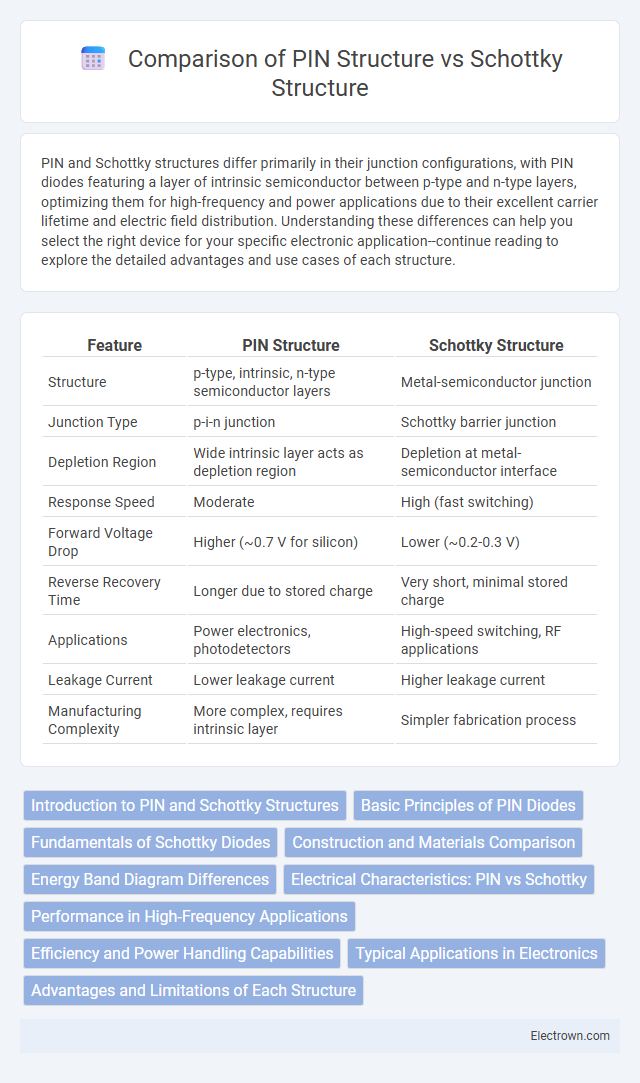
| Feature | PIN Structure | Schottky Structure |
|---|---|---|
| Structure | p-type, intrinsic, n-type semiconductor layers | Metal-semiconductor junction |
| Junction Type | p-i-n junction | Schottky barrier junction |
| Depletion Region | Wide intrinsic layer acts as depletion region | Depletion at metal-semiconductor interface |
| Response Speed | Moderate | High (fast switching) |
| Forward Voltage Drop | Higher (~0.7 V for silicon) | Lower (~0.2-0.3 V) |
| Reverse Recovery Time | Longer due to stored charge | Very short, minimal stored charge |
| Applications | Power electronics, photodetectors | High-speed switching, RF applications |
| Leakage Current | Lower leakage current | Higher leakage current |
| Manufacturing Complexity | More complex, requires intrinsic layer | Simpler fabrication process |
Introduction to PIN and Schottky Structures
PIN and Schottky structures represent two distinct configurations in semiconductor devices with unique characteristics influencing their applications. A PIN structure consists of an intrinsic layer sandwiched between p-type and n-type regions, enhancing performance in high-frequency and photodetector devices due to its wide depletion region and high breakdown voltage. The Schottky structure, formed by metal-semiconductor junctions, offers faster switching speeds and lower forward voltage drop, making it ideal for high-speed rectifiers and RF applications.
Basic Principles of PIN Diodes
PIN diodes consist of an intrinsic semiconductor layer sandwiched between p-type and n-type regions, allowing efficient control of current flow and high-frequency switching. The intrinsic layer in PIN diodes creates a wide depletion region that enhances carrier storage and reduces capacitance, improving performance in RF and microwave applications. You benefit from the PIN structure's ability to handle high voltage and power levels compared to the Schottky diode, which relies on a metal-semiconductor junction for faster switching but with lower voltage tolerance.
Fundamentals of Schottky Diodes
Schottky diodes feature a metal-semiconductor junction, unlike PIN diodes with intrinsic layers sandwiched between p-type and n-type regions, enabling faster switching speeds and lower forward voltage drops. The metal-semiconductor interface forms a Schottky barrier that controls charge carrier flow, resulting in minimal charge storage and reduced recovery time. These fundamental properties make Schottky diodes ideal for high-frequency and low-power applications where efficiency and rapid response are critical.
Construction and Materials Comparison
The PIN diode structure consists of an intrinsic layer sandwiched between p-type and n-type semiconductor materials, typically silicon, to enhance its voltage and power handling capabilities. In contrast, the Schottky diode structure features a metal-semiconductor junction formed by a metal contact on an n-type semiconductor, usually silicon or gallium arsenide, enabling faster switching speeds. While PIN diodes use a depletion region in the intrinsic layer for charge storage, Schottky diodes rely on majority carriers and a low forward voltage drop due to their metal-semiconductor interface.
Energy Band Diagram Differences
The energy band diagram of a PIN structure features an intrinsic layer between the p-type and n-type regions, creating a wide depletion zone that enhances charge carrier separation and reduces recombination. In contrast, the Schottky structure exhibits a metal-semiconductor junction with a distinct Schottky barrier height formed at the interface, resulting in a narrower depletion region and faster carrier transport. Understanding these differences in energy band alignments helps you optimize device performance for specific applications such as photodetectors or high-speed diodes.
Electrical Characteristics: PIN vs Schottky
PIN diodes exhibit high reverse breakdown voltage and low leakage current due to their intrinsic layer, making them ideal for high-voltage and high-frequency applications. Schottky diodes show low forward voltage drop (typically 0.2-0.3 V) and fast switching speed, but have lower reverse breakdown voltage and higher leakage current compared to PIN diodes. Your choice between PIN and Schottky structures depends on whether you prioritize efficiency and speed over voltage tolerance and leakage performance.
Performance in High-Frequency Applications
PIN diodes exhibit superior performance in high-frequency applications due to their intrinsic layer, which reduces capacitance and enhances switching speed, making them ideal for RF switches and attenuators. Schottky diodes, characterized by low forward voltage drop and fast recovery time, excel in high-frequency rectification but suffer from higher junction capacitance compared to PIN diodes. The low series resistance and quick response of Schottky diodes improve efficiency in mixer circuits, while PIN diodes offer better linearity and power handling in microwave frequency ranges.
Efficiency and Power Handling Capabilities
PIN diodes offer higher efficiency and superior power handling capabilities due to their intrinsic layer, which allows for better voltage distribution and reduced carrier recombination, making them ideal for high-frequency and high-power applications. Schottky diodes, while faster with lower forward voltage drops, exhibit lower efficiency and limited power handling due to their metal-semiconductor junction, which results in higher leakage currents and reduced thermal stability. Your choice depends on the required balance between switching speed and power efficiency for specific electronic circuit demands.
Typical Applications in Electronics
PIN diode structures are commonly used in RF switches, photodetectors, and high-voltage power electronics due to their ability to sustain high reverse voltages and efficiently handle high-frequency signals. Schottky diodes find typical applications in power rectifiers, radio frequency mixers, and clamping circuits because of their low forward voltage drop and fast switching speed. Your choice between PIN and Schottky structures depends on application requirements such as voltage handling, switching speed, and power efficiency.
Advantages and Limitations of Each Structure
PIN diode structures offer high breakdown voltage and low capacitance, making them suitable for high-frequency and high-power applications, but suffer from slower switching speeds due to minority carrier storage. Schottky diode structures provide ultra-fast switching and low forward voltage drop, enhancing efficiency in high-speed circuits, yet they have lower voltage handling capability and higher reverse leakage current. The choice between PIN and Schottky depends on the specific requirements for speed, voltage, and power efficiency in electronic designs.
PIN structure vs Schottky structure Infographic