Photonic crystals offer superior control over light propagation by exploiting periodic dielectric structures that create photonic band gaps, unlike conventional waveguides that rely on total internal reflection within uniform media. Explore the rest of this article to understand how your choices in waveguide technology can impact optical performance and application suitability.
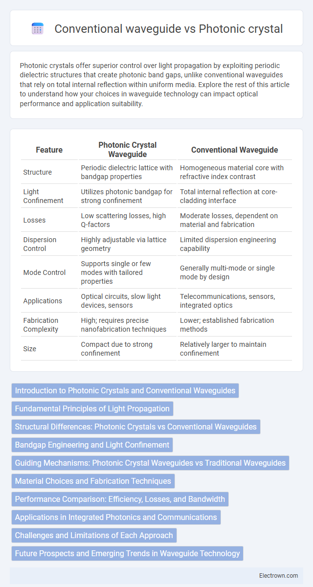
Table of Comparison
| Feature | Photonic Crystal Waveguide | Conventional Waveguide |
|---|---|---|
| Structure | Periodic dielectric lattice with bandgap properties | Homogeneous material core with refractive index contrast |
| Light Confinement | Utilizes photonic bandgap for strong confinement | Total internal reflection at core-cladding interface |
| Losses | Low scattering losses, high Q-factors | Moderate losses, dependent on material and fabrication |
| Dispersion Control | Highly adjustable via lattice geometry | Limited dispersion engineering capability |
| Mode Control | Supports single or few modes with tailored properties | Generally multi-mode or single mode by design |
| Applications | Optical circuits, slow light devices, sensors | Telecommunications, sensors, integrated optics |
| Fabrication Complexity | High; requires precise nanofabrication techniques | Lower; established fabrication methods |
| Size | Compact due to strong confinement | Relatively larger to maintain confinement |
Introduction to Photonic Crystals and Conventional Waveguides
Photonic crystals are materials with periodic dielectric structures that manipulate light propagation through photonic band gaps, enabling precise control of optical signals. Conventional waveguides, typically made of homogeneous materials like silica or silicon, confine light by total internal reflection within a core surrounded by cladding. Unlike conventional waveguides, photonic crystals utilize their periodic lattice to guide light with reduced losses and enhanced dispersion control, crucial for advanced optical communication and sensing applications.
Fundamental Principles of Light Propagation
Photonic crystals utilize periodic dielectric structures to create photonic band gaps that control and confine light propagation through Bragg scattering, enabling highly efficient and wavelength-selective guidance. Conventional waveguides rely on total internal reflection caused by the refractive index contrast between the core and cladding, guiding light through continuous refractive index boundaries. The fundamental difference lies in photonic crystals manipulating light via bandgap effects while conventional waveguides depend on total internal reflection for light confinement.
Structural Differences: Photonic Crystals vs Conventional Waveguides
Photonic crystals feature periodic dielectric structures that manipulate light through photonic band gaps, while conventional waveguides rely on total internal reflection within homogeneous or layered materials. The periodicity in photonic crystals creates wavelength-specific control and confinement of light, enabling unique dispersion properties not achievable in traditional waveguides. Your choice between these depends on the need for engineered light propagation versus straightforward guiding with minimal structural complexity.
Bandgap Engineering and Light Confinement
Photonic crystal waveguides use periodic dielectric structures to create photonic bandgaps that precisely control light propagation, enabling superior light confinement and reduced scattering losses compared to conventional waveguides. In contrast, conventional waveguides rely on total internal reflection with refractive index contrast, limiting their ability to engineer photonic bandgaps and often resulting in higher propagation losses. Leveraging bandgap engineering in photonic crystals allows your optical devices to achieve enhanced performance, including tighter mode confinement and improved control over light flow at the nanoscale.
Guiding Mechanisms: Photonic Crystal Waveguides vs Traditional Waveguides
Photonic crystal waveguides guide light using periodic dielectric structures that create photonic bandgaps, enabling tight confinement and low-loss propagation even around sharp bends. Conventional waveguides rely on total internal reflection in a high-refractive-index core surrounded by lower-index cladding, often limiting bending performance and integration density. Your optical system can benefit from photonic crystal waveguides when requiring precise light control with minimal scattering compared to traditional waveguide designs.
Material Choices and Fabrication Techniques
Photonic crystals utilize periodic dielectric materials such as silicon, gallium arsenide, or silicon nitride to manipulate light propagation through bandgap engineering, whereas conventional waveguides commonly employ homogeneous materials like silica or polymer-based substrates. Fabrication of photonic crystals involves advanced techniques including electron-beam lithography, reactive ion etching, and focused ion beam milling to create nanoscale periodic structures with high precision. In contrast, conventional waveguide fabrication typically relies on chemical vapor deposition, photolithography, and wet or dry etching processes optimized for smoother, larger-scale interfaces.
Performance Comparison: Efficiency, Losses, and Bandwidth
Photonic crystal waveguides exhibit superior performance in efficiency by enabling tight light confinement, resulting in lower propagation losses compared to conventional waveguides. Their engineered bandgap structures support broader bandwidth and reduced scattering, enhancing signal integrity in optical communication. Conventional waveguides, while simpler and cost-effective, generally experience higher attenuation and limited bandwidth due to material and geometric constraints.
Applications in Integrated Photonics and Communications
Photonic crystals enable ultra-compact and low-loss light manipulation in integrated photonics, enhancing on-chip optical signal processing and filtering with subwavelength confinement. Conventional waveguides, such as silicon or silica-based, provide robust, broadband transmission for optical interconnects and fiber-to-chip coupling widely used in telecommunications. The photonic crystal's ability to engineer bandgaps and dispersion properties offers customizable wavelength multiplexing and sensing applications beyond conventional waveguides' capabilities.
Challenges and Limitations of Each Approach
Photonic crystal waveguides face challenges such as fabrication complexity and sensitivity to structural imperfections, which can lead to scattering losses and reduced performance. Conventional waveguides encounter limitations in miniaturization due to diffraction limits and higher propagation losses at sharp bends. Both approaches struggle with integration into compact photonic circuits, necessitating trade-offs between loss, size, and manufacturing scalability.
Future Prospects and Emerging Trends in Waveguide Technology
Photonic crystal waveguides offer unprecedented control over light propagation through engineered bandgaps, enabling ultra-compact and low-loss devices surpassing conventional waveguides. Emerging trends include integration with silicon photonics for scalable on-chip optical circuits and the development of tunable photonic crystals for dynamic signal manipulation. Your future applications benefit from these advances, promising enhanced performance in optical communications, sensing, and quantum information processing.
Photonic crystal vs Conventional waveguide Infographic