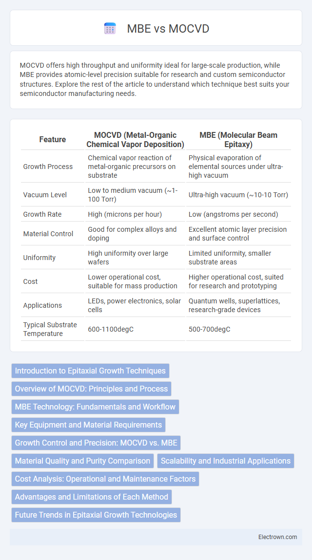
MOCVD offers high throughput and uniformity ideal for large-scale production, while MBE provides atomic-level precision suitable for research and custom semiconductor structures. Explore the rest of the article to understand which technique best suits your semiconductor manufacturing needs.
Table of Comparison
| Feature | MOCVD (Metal-Organic Chemical Vapor Deposition) | MBE (Molecular Beam Epitaxy) |
|---|---|---|
| Growth Process | Chemical vapor reaction of metal-organic precursors on substrate | Physical evaporation of elemental sources under ultra-high vacuum |
| Vacuum Level | Low to medium vacuum (~1-100 Torr) | Ultra-high vacuum (~10-10 Torr) |
| Growth Rate | High (microns per hour) | Low (angstroms per second) |
| Material Control | Good for complex alloys and doping | Excellent atomic layer precision and surface control |
| Uniformity | High uniformity over large wafers | Limited uniformity, smaller substrate areas |
| Cost | Lower operational cost, suitable for mass production | Higher operational cost, suited for research and prototyping |
| Applications | LEDs, power electronics, solar cells | Quantum wells, superlattices, research-grade devices |
| Typical Substrate Temperature | 600-1100degC | 500-700degC |
Introduction to Epitaxial Growth Techniques
Metal-Organic Chemical Vapor Deposition (MOCVD) and Molecular Beam Epitaxy (MBE) are two prominent epitaxial growth techniques used for fabricating high-quality semiconductor layers. MOCVD involves the chemical vapor deposition of metal-organic precursors at elevated temperatures, enabling large-area uniformity and scalability for devices like LEDs and solar cells. MBE utilizes ultra-high vacuum and atomic or molecular beams for layer-by-layer crystal growth with precise control over thickness and composition, ideal for quantum wells and advanced electronic structures.
Overview of MOCVD: Principles and Process
Metal-Organic Chemical Vapor Deposition (MOCVD) utilizes volatile metal-organic precursors and hydrides to deposit epitaxial layers on substrates through chemical reactions at elevated temperatures. The process involves gas-phase transport, adsorption, surface reactions, and film growth, enabling precise control over composition, thickness, and doping in semiconductor fabrication. MOCVD is widely favored for high-throughput production of compound semiconductors such as GaN, InP, and related alloys, supporting applications in LEDs, lasers, and power devices.
MBE Technology: Fundamentals and Workflow
Molecular Beam Epitaxy (MBE) technology operates under ultra-high vacuum conditions to precisely deposit atomic layers, enabling superior control over film thickness and composition at the nanoscale. Its workflow involves generating molecular beams from effusion cells, directing them onto a heated substrate where epitaxial growth occurs, and real-time monitoring via reflection high-energy electron diffraction (RHEED) to ensure layer-by-layer control. Compared to Metal-Organic Chemical Vapor Deposition (MOCVD), MBE offers enhanced precision for fabricating complex quantum structures despite lower throughput and slower growth rates.
Key Equipment and Material Requirements
MOCVD (Metal-Organic Chemical Vapor Deposition) requires complex gas delivery systems and precursors such as metal-organic compounds, necessitating high-purity sources and precise temperature control for uniform thin-film growth. MBE (Molecular Beam Epitaxy) relies on ultra-high vacuum chambers equipped with effusion cells for evaporating elemental sources, demanding extremely clean environments and precise flux monitoring to achieve atomically controlled layers. Your choice between these techniques hinges on the specific material systems and device structures, with MOCVD favoring large-scale production and MBE excelling in atomic-scale precision.
Growth Control and Precision: MOCVD vs. MBE
MOCVD offers high growth rates with excellent uniformity, making it ideal for large-scale semiconductor manufacturing, while MBE provides unparalleled atomic-level precision and layer-by-layer control essential for research and advanced device fabrication. Your choice depends on the required growth control, with MBE excelling in ultra-thin film deposition and precise interface engineering, whereas MOCVD excels in scalability and reproducibility. Both techniques deliver excellent crystalline quality but differ significantly in process complexity and control granularity.
Material Quality and Purity Comparison
Molecular Beam Epitaxy (MBE) offers superior material quality and atomic-level precision, yielding ultra-pure and defect-free epitaxial layers ideal for research and high-performance devices. Metal-Organic Chemical Vapor Deposition (MOCVD) provides scalable growth with excellent uniformity and high throughput, though it may introduce more impurities due to precursor chemistry. MBE's ultra-high vacuum environment ensures higher purity, while MOCVD's chemical precursors can result in trace contamination affecting semiconductor interface quality.
Scalability and Industrial Applications
MOCVD offers superior scalability due to its high throughput and ability to grow uniform thin films over large wafer sizes, making it ideal for mass production in the semiconductor and LED industries. MBE provides precise atomic layer control, crucial for research and specialized devices but faces limitations in scalability and throughput, restricting its use primarily to niche applications. Your choice between MOCVD and MBE depends on whether industrial-scale manufacturing or atomic-scale precision is the priority.
Cost Analysis: Operational and Maintenance Factors
Metal-Organic Chemical Vapor Deposition (MOCVD) typically incurs lower operational costs due to its higher throughput and efficient precursor usage, whereas Molecular Beam Epitaxy (MBE) requires more expensive ultra-high vacuum equipment and maintenance. Maintenance for MBE often involves complex vacuum system upkeep and frequent chamber bake-outs, driving up downtime and costs compared to MOCVD's more straightforward gas delivery system servicing. Cost efficiency in MOCVD is further enhanced by automated wafer handling and quicker cycle times, making it preferable for large-scale commercial semiconductor manufacturing.
Advantages and Limitations of Each Method
Metal-Organic Chemical Vapor Deposition (MOCVD) offers high growth rates and excellent uniformity, making it ideal for mass production of semiconductor devices, but it can introduce impurities due to precursor decomposition. Molecular Beam Epitaxy (MBE) provides superior control over atomic layer deposition and surface morphology, essential for research and precise heterostructure fabrication, yet it operates at slower growth rates and higher costs. Your choice depends on whether you prioritize scalability and speed with MOCVD or atomic-level precision and customization with MBE.
Future Trends in Epitaxial Growth Technologies
Future trends in epitaxial growth technologies emphasize advancements in Metalorganic Chemical Vapor Deposition (MOCVD) and Molecular Beam Epitaxy (MBE) to achieve higher precision and scalability for next-generation semiconductors. MOCVD developments focus on enhancing deposition rates and uniformity for large-scale production of III-V compound semiconductors used in optoelectronics and power devices. MBE continues to evolve with atomic layer control and in-situ monitoring to enable complex quantum structures and two-dimensional materials critical for quantum computing and advanced electronic applications.
MOCVD vs MBE Infographic