MOCVD offers precise control over thin film deposition with excellent uniformity, making it ideal for complex semiconductor devices, while HVPE excels in high growth rates and cost-effective production of thick epitaxial layers. Explore the detailed comparison to understand which technique best suits your advanced material growth needs.
Table of Comparison
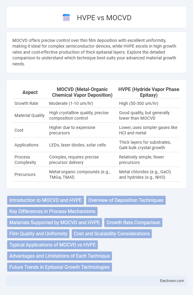
| Aspect | MOCVD (Metal-Organic Chemical Vapor Deposition) | HVPE (Hydride Vapor Phase Epitaxy) |
|---|---|---|
| Growth Rate | Moderate (1-10 um/hr) | High (50-300 um/hr) |
| Material Quality | High crystalline quality, precise composition control | Good quality, but generally lower than MOCVD |
| Cost | Higher due to expensive precursors | Lower, uses simpler gases like HCl and metal |
| Applications | LEDs, laser diodes, solar cells | Thick layers for substrates, GaN bulk crystal growth |
| Process Complexity | Complex, requires precise precursor delivery | Relatively simple, fewer precursors |
| Precursors | Metal-organic compounds (e.g., TMGa, TMAl) | Metal chlorides (e.g., GaCl) and hydrides (e.g., NH3) |
Introduction to MOCVD and HVPE
Metalorganic Chemical Vapor Deposition (MOCVD) and Hydride Vapor Phase Epitaxy (HVPE) are advanced techniques for growing high-quality semiconductor crystals. MOCVD uses metalorganic compounds and gas-phase reactions to deposit thin films with precise control over composition and thickness, ideal for complex device structures. HVPE offers rapid growth rates by reacting metal chlorides with hydride gases, making it suitable for large-volume production of bulk materials like GaN and other III-V semiconductors.
Overview of Deposition Techniques
Metal-Organic Chemical Vapor Deposition (MOCVD) utilizes metal-organic precursors and hydrides to deposit thin films with precise compositional control, making it ideal for complex semiconductors and multi-layer structures. Hydride Vapor Phase Epitaxy (HVPE) relies on the reaction of metal chlorides with hydrides at high temperatures, enabling rapid growth rates and high purity films primarily suited for bulk GaN substrates. Both techniques are pivotal in semiconductor manufacturing, with MOCVD favored for device heterostructures and HVPE optimized for thick layer deposition.
Key Differences in Process Mechanisms
MOCVD (Metal-Organic Chemical Vapor Deposition) utilizes metal-organic precursors decomposed on a heated substrate to form thin films with precise compositional control, making it ideal for complex semiconductor structures. HVPE (Hydride Vapor Phase Epitaxy) relies on the reaction of gaseous metal chlorides and hydrides, offering faster growth rates but less fine compositional control compared to MOCVD. Your choice between these methods depends on the trade-off between the speed and complexity of the epitaxial layer formation required for your application.
Materials Supported by MOCVD and HVPE
MOCVD supports a wide range of materials including III-V semiconductors such as GaAs, InP, and GaN, as well as complex oxides and nitrides used in optoelectronic and power devices. HVPE excels in growing thick GaN layers and other III-nitride materials with high growth rates, making it suitable for substrates and buffer layers in LED and high-electron-mobility transistor (HEMT) production. Both techniques cater to different material demands, with MOCVD favoring device-quality epitaxial layers and HVPE offering rapid bulk crystal growth.
Growth Rate Comparison
Metal-Organic Chemical Vapor Deposition (MOCVD) typically achieves growth rates ranging from 1 to 10 micrometers per hour, making it suitable for precise thin-film applications. Hydride Vapor Phase Epitaxy (HVPE) offers significantly higher growth rates, often exceeding 100 micrometers per hour, which is advantageous for thick layer deposition. The stark contrast in growth rates stems from HVPE's use of gaseous hydrides enabling faster precursor supply and reaction kinetics compared to the metal-organic precursors in MOCVD.
Film Quality and Uniformity
MOCVD (Metal-Organic Chemical Vapor Deposition) produces films with superior uniformity and high crystalline quality due to precise precursor control and lower growth temperatures, making it ideal for complex heterostructures. HVPE (Hydride Vapor Phase Epitaxy) typically yields thicker films with good crystalline quality but exhibits less uniformity over large wafers, often facing challenges in defect density and surface smoothness. The choice between MOCVD and HVPE depends on application requirements, with MOCVD preferred for high-precision semiconductor devices and HVPE favored for rapid thick film growth.
Cost and Scalability Considerations
MOCVD systems typically involve higher equipment and operational costs due to complex precursor gases and precise process control requirements, whereas HVPE offers a more cost-effective solution with lower material expenses and simpler hardware. Scalability in MOCVD is often limited by slower growth rates and higher maintenance demands, while HVPE enables faster layer deposition, making it more suitable for large-scale production of thick epitaxial layers. Your choice between these methods should weigh initial investment against long-term throughput needs and product specifications.
Typical Applications of MOCVD vs HVPE
MOCVD is widely used for fabricating high-quality semiconductor devices such as LEDs, laser diodes, and solar cells due to its precise control over thin film composition and thickness. HVPE excels in producing bulk GaN substrates and thick epitaxial layers rapidly, making it ideal for applications requiring large-area or high-volume GaN wafers like power electronics and LED substrate manufacturing. Your choice between MOCVD and HVPE depends on whether you prioritize thin film precision or high growth rates for bulk material production.
Advantages and Limitations of Each Technique
MOCVD offers precise control over composition and uniformity, enabling high-quality thin films ideal for complex semiconductor devices, but it involves higher operational costs and slower growth rates. HVPE provides rapid growth rates and cost-effective production suited for bulk layers and large-area substrates, yet it lacks the fine compositional control and uniformity achieved by MOCVD. Each technique balances speed, cost, and material quality, influencing their suitability for specific applications in compound semiconductor manufacturing.
Future Trends in Epitaxial Growth Technologies
Future trends in epitaxial growth technologies highlight MOCVD's increasing adoption due to its precise control over layer thickness and composition for advanced semiconductor devices. HVPE remains valuable for high-volume, cost-effective production of thick GaN layers, supporting substrate manufacturing for power electronics. Your choice between MOCVD and HVPE will depend on balancing scalability with material quality as both technologies evolve toward faster growth rates and improved uniformity.
MOCVD vs HVPE Infographic