Epitaxial growth enables precise layering of semiconductor materials with controlled thickness and composition, essential for fabricating high-performance devices. You can discover how ion-implantation complements this process by modifying electrical properties, enhancing your understanding of advanced semiconductor fabrication techniques in the rest of the article.
Table of Comparison
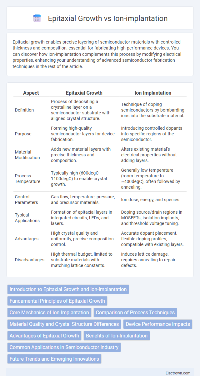
| Aspect | Epitaxial Growth | Ion Implantation |
|---|---|---|
| Definition | Process of depositing a crystalline layer on a semiconductor substrate with aligned crystal structure. | Technique of doping semiconductors by bombarding ions into the substrate material. |
| Purpose | Forming high-quality semiconductor layers for device fabrication. | Introducing controlled dopants into specific regions of the semiconductor. |
| Material Modification | Adds new material layers with precise thickness and composition. | Alters existing material's electrical properties without adding layers. |
| Process Temperature | Typically high (600degC-1100degC) to enable crystal growth. | Generally low temperature (room temperature to ~400degC), often followed by annealing. |
| Control Parameters | Gas flow, temperature, pressure, and precursor materials. | Ion dose, energy, and species. |
| Typical Applications | Formation of epitaxial layers in integrated circuits, LEDs, and lasers. | Doping source/drain regions in MOSFETs, isolation implants, and threshold voltage tuning. |
| Advantages | High crystal quality and uniformity, precise composition control. | Accurate dopant placement, flexible doping profiles, compatible with existing layers. |
| Disadvantages | High thermal budget, limited to substrate materials with matching lattice constants. | Induces lattice damage, requires annealing to repair defects. |
Introduction to Epitaxial Growth and Ion-Implantation
Epitaxial growth involves the deposition of a crystalline layer on a semiconductor substrate, preserving the atomic arrangement for high-quality material fabrication essential in microelectronics. Ion-implantation introduces dopants into the substrate through accelerated ion beams, allowing precise control of dopant concentration and depth in semiconductor devices. Both techniques are fundamental in semiconductor manufacturing, with epitaxial growth enhancing crystal quality and ion-implantation enabling targeted electrical property modifications.
Fundamental Principles of Epitaxial Growth
Epitaxial growth involves depositing a crystalline layer on a substrate crystal, ensuring the deposited film inherits the substrate's lattice structure and orientation, which is crucial for high-quality semiconductor device fabrication. This process relies on mechanisms such as molecular beam epitaxy (MBE) or chemical vapor deposition (CVD) to precisely control atomic layer arrangement, enabling superior electrical properties in materials like silicon or gallium arsenide. Your choice of epitaxial growth over ion implantation can significantly impact device performance by minimizing crystal damage and preserving carrier mobility in the semiconductor lattice.
Core Mechanics of Ion-Implantation
Ion-implantation involves accelerating ions of a desired element into a semiconductor substrate to alter its physical, chemical, or electrical properties by introducing dopants at controlled depths and concentrations. The core mechanics center on ion acceleration using electric fields, beam collimation, and precise dosage control to achieve uniform implantation profiles. Unlike epitaxial growth, which builds layers atom-by-atom, ion-implantation modifies the substrate lattice through collision and substitution processes, enabling localized doping without changing the surface topography significantly.
Comparison of Process Techniques
Epitaxial growth involves the deposition of a crystalline layer on a semiconductor substrate, enabling precise control over thickness, doping profiles, and crystal quality, which is essential for high-performance devices. Ion implantation introduces dopants into the substrate by accelerating ions into the material, allowing for localized doping with controlled depth and concentration but often requiring subsequent annealing to repair lattice damage. Both techniques are critical in semiconductor fabrication, with epitaxial growth favored for forming uniform, defect-free layers, while ion implantation provides flexibility in doping patterns for complex integrated circuits.
Material Quality and Crystal Structure Differences
Epitaxial growth produces high-quality, single-crystal layers that maintain the substrate's crystal structure, resulting in minimal defects and superior electrical properties. Ion implantation introduces dopants by bombarding the substrate with ions, often causing crystal lattice damage and defects that require annealing to partially restore material quality. Consequently, epitaxial growth is preferred for applications demanding pristine crystal structures, while ion implantation offers precise doping control at the cost of potential crystal disruption.
Device Performance Impacts
Epitaxial growth produces high-quality crystalline layers that enhance carrier mobility and reduce defect densities, significantly improving device efficiency and performance. Ion implantation introduces dopants precisely but can induce lattice damage, requiring annealing to restore crystal quality and minimize performance degradation. You can achieve optimal device characteristics by carefully selecting epitaxial growth for superior layer uniformity or ion implantation for precise doping control, depending on the application needs.
Advantages of Epitaxial Growth
Epitaxial growth offers precise control over the thickness and composition of semiconductor layers, enabling high-quality crystalline films with minimal defects essential for advanced electronic and optoelectronic devices. This method provides superior interface quality and abrupt junctions compared to ion-implantation, which often causes lattice damage requiring subsequent annealing. High electron mobility and improved carrier concentration uniformity are additional advantages of epitaxial layers, enhancing device performance in applications like high-speed transistors and laser diodes.
Benefits of Ion-Implantation
Ion-implantation offers precise control over dopant concentration and depth profiles in semiconductor materials, enabling tailored electrical properties with minimal damage to the crystal lattice. This technique provides high spatial resolution for localized doping, essential for advanced microelectronics and nanoscale device fabrication. Ion-implantation also allows for low-temperature processing, reducing thermal budgets and preserving underlying layers compared to traditional epitaxial growth methods.
Common Applications in Semiconductor Industry
Epitaxial growth is widely used in producing high-quality semiconductor layers for advanced devices like high-electron-mobility transistors (HEMTs) and photovoltaic cells, ensuring precise control over crystal structure and doping profiles. Ion implantation enables localized doping of semiconductor substrates, crucial for fabricating integrated circuits, MOSFETs, and CMOS technology by introducing impurities at specific depths with high accuracy. Both techniques complement each other in semiconductor manufacturing to optimize performance, reliability, and scalability across microelectronics and optoelectronic applications.
Future Trends and Emerging Innovations
Epitaxial growth is advancing through atomic layer deposition and selective area epitaxy, enabling ultra-thin, defect-free semiconductor layers critical for next-generation transistors and quantum computing devices. Ion-implantation innovations focus on precise dopant placement using advanced masking and in-situ annealing techniques, enhancing device performance and scalability for 5G and beyond. Both methods are integrating machine learning algorithms for process optimization, driving higher throughput and reduced variability in semiconductor manufacturing.
Epitaxial growth vs Ion-implantation Infographic