Si photonics offers cost-effective integration with existing CMOS technology, enabling high-density, scalable optical communication solutions, while III-V photonics provides superior performance in light emission and amplification due to direct bandgap materials. Explore the rest of the article to understand how choosing between Si and III-V photonics can impact Your photonic device design and application outcomes.
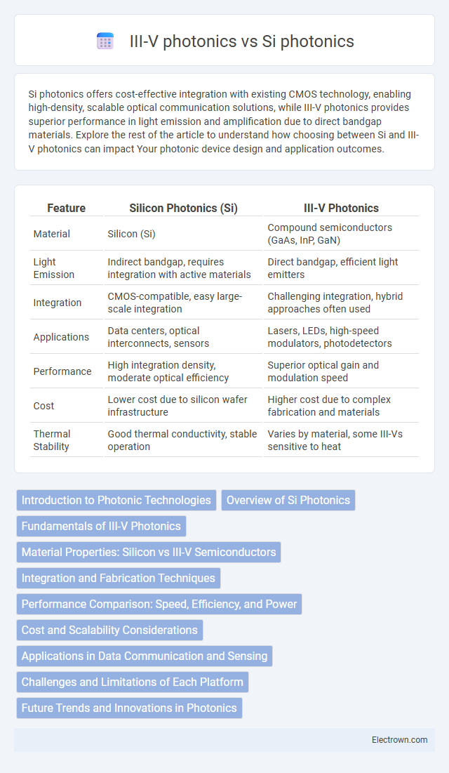
Table of Comparison
| Feature | Silicon Photonics (Si) | III-V Photonics |
|---|---|---|
| Material | Silicon (Si) | Compound semiconductors (GaAs, InP, GaN) |
| Light Emission | Indirect bandgap, requires integration with active materials | Direct bandgap, efficient light emitters |
| Integration | CMOS-compatible, easy large-scale integration | Challenging integration, hybrid approaches often used |
| Applications | Data centers, optical interconnects, sensors | Lasers, LEDs, high-speed modulators, photodetectors |
| Performance | High integration density, moderate optical efficiency | Superior optical gain and modulation speed |
| Cost | Lower cost due to silicon wafer infrastructure | Higher cost due to complex fabrication and materials |
| Thermal Stability | Good thermal conductivity, stable operation | Varies by material, some III-Vs sensitive to heat |
Introduction to Photonic Technologies
Silicon photonics exploits silicon's mature CMOS fabrication for cost-effective, high-density optical components primarily used in data communications and interconnects. III-V photonics employs compound semiconductors like gallium arsenide and indium phosphide, offering superior direct bandgap properties essential for efficient light emission and laser integration. Both technologies drive advances in photonic integrated circuits, balancing silicon's scalability with III-V materials' optoelectronic performance.
Overview of Si Photonics
Silicon photonics leverages silicon's well-established CMOS fabrication technology to integrate optical components with electronic circuits on a single chip, enabling high-volume, low-cost production. The platform excels in data communication applications due to its compatibility with silicon-based electronics and strong potential for dense integration and scalability. Despite silicon's indirect bandgap limiting efficient light emission, advances in heterogeneous integration and novel light sources are expanding its capabilities.
Fundamentals of III-V Photonics
III-V photonics relies on compound semiconductors such as gallium arsenide (GaAs) and indium phosphide (InP), which possess direct bandgaps enabling efficient light emission and detection. These materials exhibit superior optoelectronic properties for laser diodes, modulators, and photodetectors compared to silicon's indirect bandgap, making them ideal for active photonic components. III-V photonics enables integration of high-speed and high-efficiency devices critical for optical communication and sensing applications.
Material Properties: Silicon vs III-V Semiconductors
Silicon photonics leverages silicon's excellent compatibility with CMOS fabrication and its strong nonlinear optical properties but suffers from an indirect bandgap, limiting efficient light emission. III-V semiconductors such as gallium arsenide (GaAs) and indium phosphide (InP) possess direct bandgaps, enabling superior light generation and detection efficiencies critical for lasers and photodetectors. Your choice between silicon and III-V materials depends on the application's requirements for integration density, optical performance, and fabrication cost.
Integration and Fabrication Techniques
Silicon photonics leverages mature CMOS fabrication processes enabling high-density integration with electronic circuits on a silicon wafer, utilizing wafer-scale fabrication and leveraging standard complementary metal-oxide-semiconductor (CMOS) foundries for cost-effective mass production. III-V photonics employs epitaxial growth techniques like molecular beam epitaxy (MBE) or metal-organic chemical vapor deposition (MOCVD) for compound semiconductor layers, often integrated heterogeneously onto silicon substrates to combine efficient light emission with silicon photonics platforms. The hybrid integration approach allows silicon photonics' scalable electronic-photonic integration to be combined with III-V materials' superior optoelectronic properties, although challenges remain in aligning lattice mismatches and thermal expansion coefficients.
Performance Comparison: Speed, Efficiency, and Power
Si photonics offers high-speed data transmission with low power consumption, ideal for large-scale integration and cost-effective applications. III-V photonics excels in efficiency and speed due to direct bandgap materials, supporting higher modulation rates and better laser performance. Your choice depends on prioritizing integration scalability with silicon or superior optical performance with III-V compounds.
Cost and Scalability Considerations
Silicon photonics offers significant cost advantages due to its compatibility with mature CMOS fabrication processes, enabling mass production and high scalability. III-V photonics, while delivering superior performance in active components like lasers and modulators, involves more complex and expensive manufacturing techniques with limited integration on silicon substrates. The scalability of silicon photonics makes it more suitable for large-volume, cost-sensitive applications, whereas III-V photonics is preferred for specialized, high-performance optical systems despite higher production costs.
Applications in Data Communication and Sensing
Silicon photonics excels in data communication due to its compatibility with CMOS manufacturing, allowing cost-effective integration of optical interconnects in data centers and telecom networks, while providing high bandwidth and low power consumption. III-V photonics, leveraging direct bandgap materials like indium phosphide, offers superior performance in sensing applications requiring high sensitivity and wavelength tunability, such as LIDAR and biosensing. Your choice between Si and III-V photonics depends on prioritizing scalability and integration versus enhanced optical functionality for specialized sensors.
Challenges and Limitations of Each Platform
Si photonics faces challenges such as inefficient light emission due to its indirect bandgap, limiting laser integration and requiring complex hybrid approaches for active components. III-V photonics offers superior light emission and gain properties but struggles with high fabrication costs, material integration complexities on silicon substrates, and thermal management issues. Your choice between these platforms depends on balancing Si photonics' scalability and cost-effectiveness against the superior optical performance but higher expense of III-V materials.
Future Trends and Innovations in Photonics
Future trends in Si photonics emphasize enhanced integration with electronics, leveraging CMOS compatibility to achieve cost-effective, scalable optical interconnects for data centers and telecommunications. III-V photonics continues to drive innovations in efficient light sources and detectors, enabling high-performance applications such as quantum computing and advanced sensing. Your choice between Si and III-V photonics will depend on the balance between integration needs and superior optical functionalities demanded by emerging technologies.
Si photonics vs III-V photonics Infographic