Plasmonic waveguides confine light beyond the diffraction limit by coupling photons with electron oscillations at metal-dielectric interfaces, enabling ultra-compact photonic circuits with high field localization. Your understanding of these differences will help you explore how each waveguide type impacts data transmission and device miniaturization; continue reading to uncover the detailed advantages and challenges of plasmonic versus photonic waveguides.
Table of Comparison
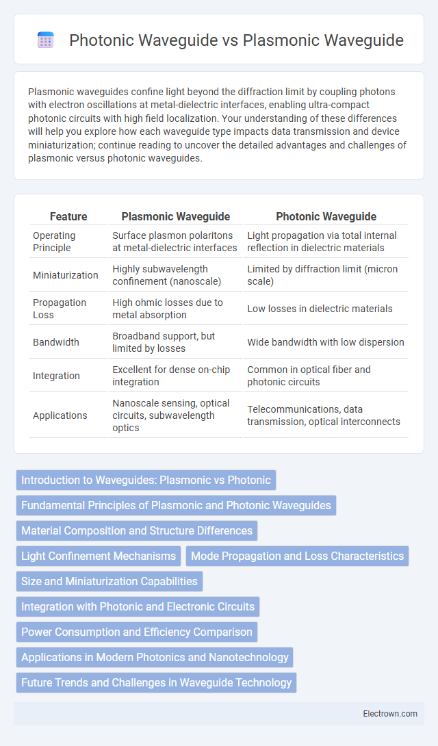
| Feature | Plasmonic Waveguide | Photonic Waveguide |
|---|---|---|
| Operating Principle | Surface plasmon polaritons at metal-dielectric interfaces | Light propagation via total internal reflection in dielectric materials |
| Miniaturization | Highly subwavelength confinement (nanoscale) | Limited by diffraction limit (micron scale) |
| Propagation Loss | High ohmic losses due to metal absorption | Low losses in dielectric materials |
| Bandwidth | Broadband support, but limited by losses | Wide bandwidth with low dispersion |
| Integration | Excellent for dense on-chip integration | Common in optical fiber and photonic circuits |
| Applications | Nanoscale sensing, optical circuits, subwavelength optics | Telecommunications, data transmission, optical interconnects |
Introduction to Waveguides: Plasmonic vs Photonic
Plasmonic waveguides exploit surface plasmon polaritons at metal-dielectric interfaces, enabling light confinement beyond the diffraction limit for ultra-compact photonic circuits. Photonic waveguides rely on total internal reflection within dielectric materials, offering low-loss signal propagation over longer distances but with larger mode volumes. The choice between plasmonic and photonic waveguides depends on trade-offs between integration density, propagation length, and fabrication complexity in optical communication systems.
Fundamental Principles of Plasmonic and Photonic Waveguides
Plasmonic waveguides operate by coupling light with free electrons at a metal-dielectric interface, generating surface plasmon polaritons that enable subwavelength light confinement beyond the diffraction limit. Photonic waveguides guide light through total internal reflection within a dielectric medium, relying on refractive index contrast to confine and direct electromagnetic waves with minimal loss. The fundamental principle difference lies in plasmonic waveguides exploiting electron oscillations for nanoscale confinement, while photonic waveguides depend on dielectric boundary conditions for efficient, low-loss propagation.
Material Composition and Structure Differences
Plasmonic waveguides utilize metals like gold or silver to confine light at the nanoscale via surface plasmon polaritons, enabling subwavelength manipulation but suffering from higher losses. Photonic waveguides rely on dielectric materials such as silicon or silica with refractive index contrast to guide light efficiently with lower attenuation but larger mode sizes. Your choice between these waveguides depends on whether nanoscale integration or low-loss propagation is the priority in your optical system design.
Light Confinement Mechanisms
Plasmonic waveguides confine light by coupling electromagnetic waves with free electrons on a metal-dielectric interface, enabling subwavelength localization beyond the diffraction limit. Photonic waveguides, in contrast, use total internal reflection within dielectric materials to guide light, resulting in confinement limited by the wavelength. Your choice between these technologies depends on the required trade-off between nanoscale confinement in plasmonics and lower propagation losses in photonics.
Mode Propagation and Loss Characteristics
Plasmonic waveguides support tightly confined surface plasmon polariton modes at metal-dielectric interfaces, enabling subwavelength mode propagation but suffer from high ohmic losses due to metal absorption. Photonic waveguides guide dielectric modes with lower propagation loss and larger mode volumes, providing efficient light transmission over longer distances. Mode confinement in plasmonic waveguides is superior for integrated nanophotonics, while photonic waveguides excel in minimizing attenuation for extended optical communication.
Size and Miniaturization Capabilities
Plasmonic waveguides enable extreme miniaturization by confining light at the nanoscale beyond the diffraction limit, making them significantly smaller than conventional photonic waveguides that are limited by the wavelength of light. While photonic waveguides typically range from hundreds of nanometers to several micrometers in size, plasmonic structures can achieve dimensions down to tens of nanometers, thus supporting ultra-compact photonic circuits. The ability of plasmonic waveguides to integrate with nanoscale electronic components positions them as a promising technology for dense on-chip optical communication systems.
Integration with Photonic and Electronic Circuits
Plasmonic waveguides enable ultra-compact integration with electronic circuits due to their ability to confine light beyond the diffraction limit, facilitating nanoscale photonic-electronic interface development. Photonic waveguides, characterized by lower loss and longer propagation distances, are widely employed in integrated photonic circuits for efficient light routing and signal processing. Combining plasmonic and photonic waveguides in hybrid systems leverages the strengths of both, optimizing overall integration density and performance in advanced photonic-electronic circuit architectures.
Power Consumption and Efficiency Comparison
Plasmonic waveguides exhibit higher power consumption due to significant ohmic losses in metal components, resulting in lower overall efficiency compared to photonic waveguides. Photonic waveguides, leveraging dielectric materials, achieve lower propagation loss, enabling more energy-efficient signal transmission over longer distances. While plasmonic waveguides offer ultra-compact device integration, their efficiency trade-offs contrast with the superior power-saving capabilities found in photonic waveguide systems.
Applications in Modern Photonics and Nanotechnology
Plasmonic waveguides enable ultra-compact photonic circuits by confining light beyond the diffraction limit, making them ideal for nanoscale optical sensors and on-chip data communication. Photonic waveguides excel in low-loss signal transmission over longer distances, supporting fiber-optic communications and integrated photonic devices. Your choice between plasmonic and photonic waveguides depends on whether device miniaturization or signal integrity is the priority in advanced nanophotonics applications.
Future Trends and Challenges in Waveguide Technology
Plasmonic waveguides offer ultra-compact integration and sub-wavelength confinement, driving future trends towards miniaturized photonic circuits, while photonic waveguides excel in low-loss transmission over longer distances, supporting high-speed data communication. Key challenges for plasmonic waveguides include managing metal-induced losses and thermal effects, whereas photonic waveguides face limitations in scalability and integration density. Advances in hybrid plasmonic-photonic structures and novel materials like graphene and transition metal dichalcogenides are pivotal for overcoming these challenges and enhancing waveguide performance.
plasmonic waveguide vs photonic waveguide Infographic