Quantum wires offer one-dimensional electron confinement, resulting in discrete energy levels along their length, while quantum ribbons provide a two-dimensional electron system with width-dependent properties affecting conductivity and optical behavior. Understanding the distinctions between these nanostructures can enhance your grasp of their applications in nanoelectronics and optoelectronics; read on to explore their unique characteristics in detail.
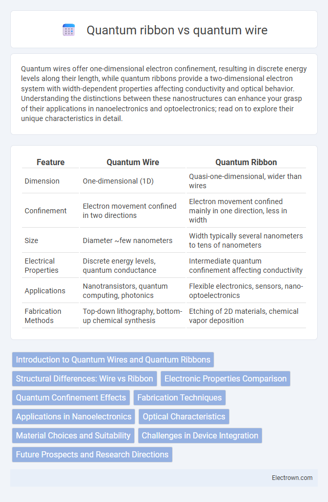
Table of Comparison
| Feature | Quantum Wire | Quantum Ribbon |
|---|---|---|
| Dimension | One-dimensional (1D) | Quasi-one-dimensional, wider than wires |
| Confinement | Electron movement confined in two directions | Electron movement confined mainly in one direction, less in width |
| Size | Diameter ~few nanometers | Width typically several nanometers to tens of nanometers |
| Electrical Properties | Discrete energy levels, quantum conductance | Intermediate quantum confinement affecting conductivity |
| Applications | Nanotransistors, quantum computing, photonics | Flexible electronics, sensors, nano-optoelectronics |
| Fabrication Methods | Top-down lithography, bottom-up chemical synthesis | Etching of 2D materials, chemical vapor deposition |
Introduction to Quantum Wires and Quantum Ribbons
Quantum wires are nanoscale structures with quantum confinement in two dimensions, allowing electron movement primarily along a single axis, resulting in discrete energy levels and enhanced electrical conductivity. Quantum ribbons, derived from two-dimensional materials like graphene, exhibit confinement in width but extended length, presenting unique edge states and tunable electronic properties. Understanding the distinctions between quantum wires and ribbons helps optimize your design choices for nanoscale electronic and photonic devices.
Structural Differences: Wire vs Ribbon
Quantum wires are one-dimensional nanostructures with a cylindrical shape that confine electrons along two dimensions, while quantum ribbons are quasi-one-dimensional materials with a rectangular cross-section, offering confinement primarily in width with extended length and width compared to wires. The structural difference impacts their electronic properties, where quantum ribbons exhibit edge effects and anisotropic conductivity due to their ribbon-like geometry. Your choice between a quantum wire and a quantum ribbon depends on the desired electron confinement and application in nanoscale devices.
Electronic Properties Comparison
Quantum wires exhibit one-dimensional electron transport with discrete energy levels, leading to enhanced quantum confinement effects and higher electron mobility compared to bulk materials. Quantum ribbons, characterized by their wider lateral dimensions, combine properties of both quantum wires and quantum wells, resulting in tunable band gaps and moderate electron mobility influenced by edge states and ribbon width. The electronic properties of quantum wires are dominated by strong quantum confinement along two dimensions, while quantum ribbons show anisotropic conductivity and variable band structure controlled by their width and edge morphology.
Quantum Confinement Effects
Quantum wires exhibit quantum confinement in two dimensions, restricting electron motion to a single axis, which significantly alters electronic and optical properties compared to bulk materials. Quantum ribbons, with confinement primarily in one dimension but extended width, display intermediate confinement effects leading to tunable bandgaps and enhanced charge carrier mobility. These quantum confinement distinctions result in varied applications in nanoelectronics and optoelectronics, where precise control of electronic states is crucial.
Fabrication Techniques
Quantum wire fabrication primarily involves top-down lithography methods such as electron beam lithography and reactive ion etching to define one-dimensional conductive paths within semiconductor materials. In contrast, quantum ribbons often utilize bottom-up growth techniques, including chemical vapor deposition (CVD) and molecular beam epitaxy (MBE), to create atomically precise, quasi-one-dimensional graphene or transition metal dichalcogenide structures. Both approaches demand nanoscale precision, but quantum ribbon synthesis emphasizes edge control and uniform width to tailor electronic properties effectively.
Applications in Nanoelectronics
Quantum wires offer superior electron confinement in one dimension, making them ideal for ultra-scaled transistors and quantum computing components, while quantum ribbons provide enhanced edge state control beneficial for spintronic devices. Both nanostructures are pivotal in developing nanoscale sensors and high-performance optoelectronic devices, leveraging their unique quantum confinement effects. The choice between quantum wires and ribbons depends on the specific application requirements in nanoelectronics, such as electron mobility and integration density.
Optical Characteristics
Quantum wires exhibit strong quantum confinement in two dimensions, leading to discrete energy levels and enhanced optical transitions characterized by sharp excitonic peaks and high photoluminescence efficiency. Quantum ribbons, with confinement primarily in one dimension, display anisotropic optical absorption and emission properties, resulting in polarization-dependent optical behavior. Both structures enable tunable optical responses crucial for applications in optoelectronics and photonic devices.
Material Choices and Suitability
Quantum wires typically utilize semiconductor materials such as InAs, GaAs, or Si to achieve one-dimensional electron confinement, optimizing their suitability for nanoelectronics and photonics applications due to high electron mobility and tunable bandgaps. Quantum ribbons, often fabricated from two-dimensional materials like graphene or transition metal dichalcogenides (TMDCs), provide enhanced edge states and tunable electronic properties, making them well-suited for spintronics and sensing devices. Material choice in quantum wires prioritizes electron transport efficiency, while quantum ribbons emphasize surface interactions and edge effects for advanced functionalization.
Challenges in Device Integration
Quantum wire and quantum ribbon technologies face significant challenges in device integration due to their distinct dimensional constraints and fabrication complexities. Quantum wires, with their one-dimensional electron transport, require precise control over size and surface defects to maintain quantum coherence, whereas quantum ribbons, offering two-dimensional confinement, demand uniform edge quality and consistent width for reliable performance. Your success in integrating these nanostructures into devices depends on overcoming issues related to scalability, material compatibility, and maintaining quantum properties during large-scale assembly.
Future Prospects and Research Directions
Quantum wires, with their one-dimensional electron transport properties, are poised to revolutionize nanoelectronics and quantum computing through enhanced electron mobility and reduced scattering. Quantum ribbons offer promising applications in spintronics due to their tunable edge states and bandgap control, enabling innovative device architectures. Current research focuses on material synthesis, interface engineering, and integration techniques to exploit quantum confinement effects for scalable, high-performance quantum devices.
quantum wire vs quantum ribbon Infographic