GaN HEMTs offer higher power density and efficiency compared to GaAs pHEMTs, making them ideal for high-frequency and high-power applications. Explore the rest of the article to understand which technology best suits your specific RF or microwave needs.
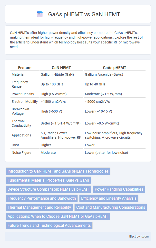
Table of Comparison
| Feature | GaN HEMT | GaAs pHEMT |
|---|---|---|
| Material | Gallium Nitride (GaN) | Gallium Arsenide (GaAs) |
| Frequency Range | Up to 100 GHz | Up to 40 GHz |
| Power Density | High (>5 W/mm) | Moderate (~1-2 W/mm) |
| Electron Mobility | ~1500 cm2/V*s | ~5000 cm2/V*s |
| Breakdown Voltage | High (>600 V) | Lower (~10-15 V) |
| Thermal Conductivity | Better (~1.3-1.4 W/cm*K) | Lower (~0.5 W/cm*K) |
| Applications | 5G, Radar, Power Amplifiers, High-power RF | Low-noise amplifiers, High-frequency switching, Microwave circuits |
| Cost | Higher | Lower |
| Noise Figure | Moderate | Lower (better for low-noise) |
Introduction to GaN HEMT and GaAs pHEMT Technologies
GaN HEMT (Gallium Nitride High Electron Mobility Transistor) and GaAs pHEMT (Gallium Arsenide pseudomorphic High Electron Mobility Transistor) are advanced semiconductor technologies used in high-frequency and power applications. GaN HEMTs offer superior power density, higher breakdown voltage, and better thermal conductivity, making them ideal for high-power RF amplifiers and switching devices. GaAs pHEMTs provide excellent electron mobility and low noise characteristics, suitable for low-noise amplifiers and sensitive RF circuits, allowing your system to optimize performance depending on power and frequency requirements.
Fundamental Material Properties: GaN vs GaAs
GaN HEMT devices leverage the wide bandgap energy of gallium nitride (3.4 eV), enabling higher breakdown voltage, greater thermal conductivity, and superior electron saturation velocity compared to GaAs pHEMTs, which have a narrower bandgap of 1.42 eV. GaAs pHEMTs benefit from mature material quality and electron mobility advantages but are limited in power density and temperature tolerance relative to GaN. Your choice between GaN and GaAs fundamentally impacts device performance in high-power, high-frequency applications.
Device Structure Comparison: HEMT vs pHEMT
GaN HEMT devices feature a wide bandgap semiconductor material with a heterojunction formed between GaN and AlGaN layers, enabling high electron mobility and superior thermal conductivity. GaAs pHEMTs utilize a pseudomorphic layer that introduces strain into the GaAs substrate, enhancing electron velocity but with lower breakdown voltage compared to GaN HEMTs. Your choice between these structures should consider the performance benefits of GaN's robust device architecture versus the mature technology and higher electron mobility offered by GaAs pHEMTs.
Power Handling Capabilities
GaN HEMT devices offer superior power handling capabilities compared to GaAs pHEMTs, with higher breakdown voltages and thermal conductivity enabling greater power density and efficiency. GaN's wide bandgap allows it to operate at higher voltages and temperatures, making it ideal for high-power RF applications. Your system can benefit from increased output power and reliability when choosing GaN HEMT for demanding power amplification tasks.
Frequency Performance and Bandwidth
GaN HEMTs exhibit superior frequency performance with cutoff frequencies (fT) often exceeding 300 GHz, compared to GaAs pHEMTs typically operating below 150 GHz, enabling higher data rates and enhanced signal integrity. The wider bandgap of GaN allows for higher breakdown voltages and greater power densities, resulting in broader operational bandwidths and improved linearity over GaAs pHEMT devices. This makes GaN HEMTs particularly advantageous for high-frequency applications such as 5G infrastructure and radar systems requiring extensive bandwidth and robust frequency response.
Efficiency and Linearity Analysis
GaN HEMT devices exhibit significantly higher efficiency and power density compared to GaAs pHEMTs due to their wider bandgap and higher breakdown voltage, enabling operation at higher voltages and frequencies. GaN HEMTs maintain superior linearity in power amplifiers, which is crucial for modern communication systems requiring high signal fidelity and low distortion. Despite GaAs pHEMT's maturity and lower noise figures, GaN technology's advancements provide enhanced performance in terms of both efficiency and linearity for RF and microwave applications.
Thermal Management and Reliability
GaN HEMTs exhibit superior thermal conductivity and higher breakdown voltage compared to GaAs pHEMTs, enabling more efficient heat dissipation and enhanced reliability under high-power and high-temperature conditions. GaN devices operate at higher junction temperatures, often exceeding 250degC, with less performance degradation, while GaAs pHEMTs typically max out around 150degC, limiting their thermal management capabilities. The wider bandgap and robust crystal structure of GaN contribute to longer device lifespan and greater tolerance to thermal cycling, making GaN HEMTs preferable for applications demanding stringent reliability and efficient thermal handling.
Cost and Manufacturing Considerations
GaN HEMTs generally incur higher manufacturing costs due to the complexity of GaN epitaxial growth and the need for specialized substrates like SiC, which offer superior thermal conductivity but elevate material expenses. In contrast, GaAs pHEMTs benefit from more mature, cost-effective fabrication processes and widespread availability of GaAs wafers, reducing overall production costs. The trade-offs between GaN's high power density and GaAs's cost efficiency significantly influence decision-making in RF power amplifier design for applications such as 5G infrastructure and radar systems.
Applications: When to Choose GaN HEMT or GaAs pHEMT
GaN HEMT devices excel in high-power, high-frequency applications such as radar systems, 5G base stations, and satellite communications due to their superior breakdown voltage and thermal conductivity. GaAs pHEMTs offer advantages in low-noise, high-frequency applications like mobile handset amplifiers and microwave communication systems, providing better noise figures and linearity. Choose GaN HEMT for power-intensive environments and GaAs pHEMT when low noise and high gain are critical to your system's performance.
Future Trends and Technological Advancements
GaN HEMT technology is rapidly advancing with superior power density, higher electron mobility, and enhanced thermal conductivity compared to GaAs pHEMT, positioning it as the preferred choice for next-generation high-frequency and high-power applications. Future trends indicate GaN HEMTs will dominate in 5G infrastructure, radar systems, and electric vehicle power electronics due to ongoing improvements in efficiency, reliability, and cost-effectiveness. Your adoption of GaN HEMT devices can leverage these technological advancements to achieve better performance and long-term scalability in emerging communication and defense systems.
GaN HEMT vs GaAs pHEMT Infographic