Floating gate and charge-trap memory technologies differ primarily in charge storage methods--floating gate stores electrons in a conductive layer, while charge-trap uses an insulating layer to trap charges, offering better scalability and reliability for advanced applications. Explore the detailed comparison to understand which technology best suits your memory design needs.
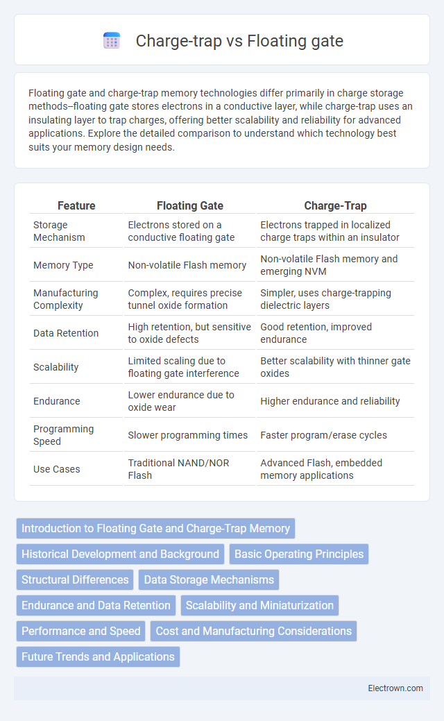
Table of Comparison
| Feature | Floating Gate | Charge-Trap |
|---|---|---|
| Storage Mechanism | Electrons stored on a conductive floating gate | Electrons trapped in localized charge traps within an insulator |
| Memory Type | Non-volatile Flash memory | Non-volatile Flash memory and emerging NVM |
| Manufacturing Complexity | Complex, requires precise tunnel oxide formation | Simpler, uses charge-trapping dielectric layers |
| Data Retention | High retention, but sensitive to oxide defects | Good retention, improved endurance |
| Scalability | Limited scaling due to floating gate interference | Better scalability with thinner gate oxides |
| Endurance | Lower endurance due to oxide wear | Higher endurance and reliability |
| Programming Speed | Slower programming times | Faster program/erase cycles |
| Use Cases | Traditional NAND/NOR Flash | Advanced Flash, embedded memory applications |
Introduction to Floating Gate and Charge-Trap Memory
Floating gate memory stores electrical charges on a conductive floating gate insulated by oxide layers, enabling non-volatile data retention commonly used in NAND flash technology. Charge-trap memory utilizes a silicon nitride or similar dielectric layer to trap charges, offering improved scalability and endurance for advanced memory applications. Your choice between these technologies depends on factors like device architecture, performance, and reliability requirements.
Historical Development and Background
Floating gate technology originated in the 1960s as the foundational design for EEPROM and flash memory, characterized by a conductive floating gate insulated by oxide layers to store charge. Charge-trap memory emerged in the 1990s as an evolution, utilizing a non-conductive dielectric layer, such as silicon nitride, to trap charges at discrete locations, offering improved scalability and reliability. The historical shift from floating gate to charge-trap reflects advancements in semiconductor fabrication and the demand for higher density, endurance, and reduced interference in non-volatile memory devices.
Basic Operating Principles
Floating gate memory stores charges in a conductive polysilicon gate insulated by oxide layers, modulating the transistor's threshold voltage to represent data. Charge-trap memory captures and retains electrons in a dielectric layer, typically silicon nitride, creating localized charge centers that alter the channel conductivity. Both technologies rely on charge storage to encode bits but utilize different materials and mechanisms to trap and isolate electrons, impacting speed, endurance, and scaling capabilities.
Structural Differences
Floating gate memory utilizes a conductive polysilicon gate completely insulated by oxide layers to store charge, enabling data retention through electron trapping within the floating gate. Charge-trap memory employs an insulating layer, typically silicon nitride, within the gate stack to capture and hold charges in discrete traps rather than a continuous conductive layer. This key structural difference influences scalability, with charge-trap devices offering improved endurance and reduced program/erase voltages compared to traditional floating gate architectures.
Data Storage Mechanisms
Floating gate memory stores data by trapping electrons on a conductive gate insulated by oxide layers, creating a stable charge that represents binary information. Charge-trap memory uses a dielectric layer, often silicon nitride, to trap charges in localized states, enabling faster program and erase cycles with improved scalability. Your choice between these mechanisms affects device endurance, data retention, and scalability in modern non-volatile memory applications.
Endurance and Data Retention
Floating gate technology offers superior data retention due to its thicker oxide layers, ensuring stable charge storage over extended periods. Charge-trap memory exhibits higher endurance, with the ability to withstand more program/erase cycles because of its insulator-based charge storage that reduces oxide degradation. Your choice depends on prioritizing long-term data stability with floating gate or enhanced write/erase cycle durability with charge-trap memory.
Scalability and Miniaturization
Floating gate technology faces challenges in scalability due to interference and charge leakage as cell sizes shrink below 20nm, limiting further miniaturization in memory devices. Charge-trap technology offers improved scalability by using thin insulating layers to trap charges, enabling smaller memory cells with better retention and endurance at advanced nodes. Your choice of memory technology should consider charge-trap's advantages in nano-scale fabrication for future-proof high-density applications.
Performance and Speed
Floating gate memory typically offers faster write and erase speeds due to its direct charge storage on a conductive gate, enabling quicker electron tunneling and improved performance for high-speed applications. Charge-trap memory, storing charge in an insulating layer, provides better scalability and endurance but generally exhibits slower write speeds due to the complex charge trapping and detrapping processes. Your choice between floating gate and charge-trap memory impacts device speed, with floating gate favoring rapid performance while charge-trap sacrifices some speed for enhanced reliability and scaling.
Cost and Manufacturing Considerations
Floating gate technology typically involves complex manufacturing steps requiring precise tunnel oxide control, which can increase production costs. Charge-trap memory uses a simpler oxide-nitride-oxide stack, reducing complexity and improving scalability, leading to lower fabrication expenses. Your choice between these technologies may impact overall cost efficiency and manufacturing yield depending on the application requirements.
Future Trends and Applications
Floating gate technology, dominant in NAND flash memory, faces scalability challenges as device dimensions shrink below 10 nm, prompting a shift toward charge-trap memory for enhanced data retention and endurance. Charge-trap memory, using silicon nitride layers to store charge, offers better resistance to leakage and improved reliability for next-generation 3D flash architectures, fueling its adoption in advanced solid-state drives and embedded non-volatile memory. Emerging applications in AI, IoT devices, and automotive systems demand high-density, low-power, and durable memory solutions, positioning charge-trap technology as a critical enabler for future semiconductor innovations.
Floating gate vs Charge-trap Infographic