Accumulation mode and inversion mode are terms often used in environmental science and meteorology to describe different atmospheric conditions affecting air pollution dispersion. Understanding how these modes influence pollutant concentration can help you better grasp air quality issues; explore the article for a detailed comparison and implications.
Table of Comparison
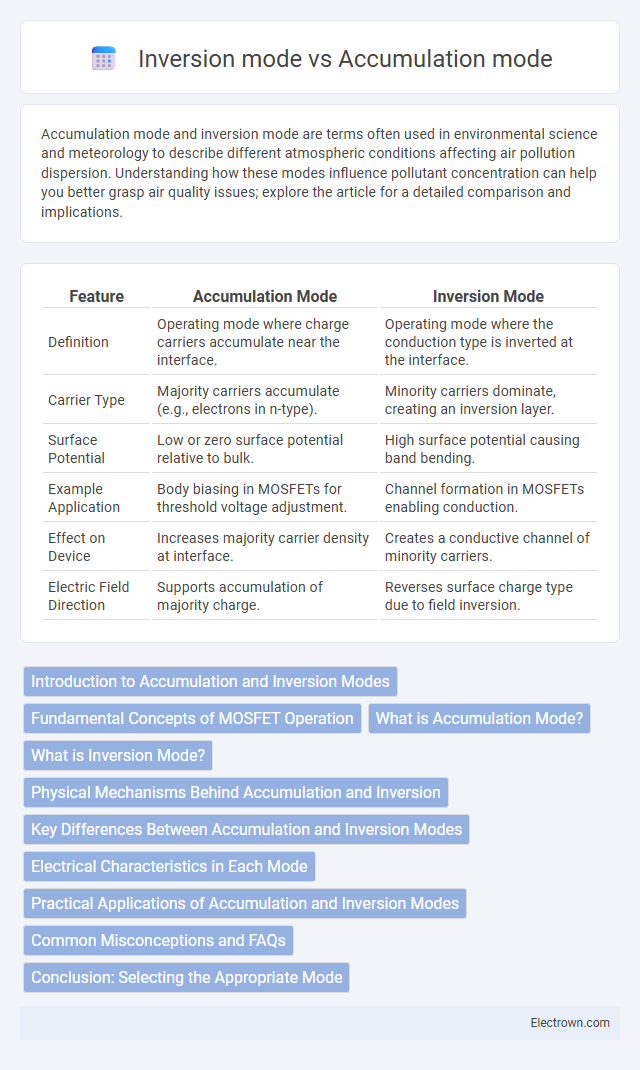
| Feature | Accumulation Mode | Inversion Mode |
|---|---|---|
| Definition | Operating mode where charge carriers accumulate near the interface. | Operating mode where the conduction type is inverted at the interface. |
| Carrier Type | Majority carriers accumulate (e.g., electrons in n-type). | Minority carriers dominate, creating an inversion layer. |
| Surface Potential | Low or zero surface potential relative to bulk. | High surface potential causing band bending. |
| Example Application | Body biasing in MOSFETs for threshold voltage adjustment. | Channel formation in MOSFETs enabling conduction. |
| Effect on Device | Increases majority carrier density at interface. | Creates a conductive channel of minority carriers. |
| Electric Field Direction | Supports accumulation of majority charge. | Reverses surface charge type due to field inversion. |
Introduction to Accumulation and Inversion Modes
Accumulation mode and inversion mode are key operating states in MOSFET devices affecting channel formation and device behavior. Accumulation mode occurs when the gate voltage attracts majority carriers, increasing surface charge density, while inversion mode happens when the gate voltage induces minority carriers, creating a conductive channel. Understanding these modes helps optimize transistor performance and tailor your semiconductor device operation.
Fundamental Concepts of MOSFET Operation
Accumulation mode in MOSFET operation occurs when a negative gate voltage causes majority carriers to gather at the semiconductor-oxide interface, increasing conductivity. Inversion mode happens when a sufficiently positive gate voltage attracts minority carriers, creating a conductive channel that allows current flow between source and drain. Understanding these fundamental concepts helps optimize your device's switching behavior and overall performance.
What is Accumulation Mode?
Accumulation mode refers to an operational state in electronic devices, particularly in MOSFETs, where a voltage applied to the gate causes majority carriers to accumulate near the semiconductor-oxide interface, increasing carrier density without forming a conductive channel. This mode contrasts with inversion mode, where minority carriers dominate the surface, creating a channel for current flow. Understanding accumulation mode helps optimize the performance of MOS devices by controlling surface charge distribution and device threshold voltage.
What is Inversion Mode?
Inversion mode is a semiconductor operation mode where the surface of a transistor channel inverts its charge type, typically forming a conductive layer of electrons in a p-type substrate for MOSFET devices. This mode enables the transistor to conduct current by creating an electric field that attracts charge carriers opposite to the substrate doping. Your understanding of inversion mode is crucial for designing efficient electronic circuits and optimizing device performance.
Physical Mechanisms Behind Accumulation and Inversion
Accumulation mode and inversion mode differ primarily in their physical mechanisms governing charge carrier distribution and energy band alignment. In accumulation mode, majority carriers increase near the semiconductor-oxide interface, caused by a negative gate voltage attracting electrons in n-type material, enhancing conductivity. In inversion mode, a sufficiently positive gate voltage induces minority carrier accumulation at the interface, creating a conducting channel of opposite carrier type through band bending and surface potential modulation.
Key Differences Between Accumulation and Inversion Modes
Accumulation mode enhances air pollutant concentrations near the surface by trapping contaminants in a stable atmospheric layer, typically under high-pressure systems, leading to poor air quality. Inversion mode occurs when a temperature inversion layer forms, where a warm air layer overlays cooler air, preventing vertical mixing and causing pollutants to accumulate close to the ground. The key difference lies in atmospheric stability: accumulation mode refers to general pollutant buildup under stagnant conditions, while inversion mode specifically involves a temperature inversion that acts as a lid, intensifying pollutant retention.
Electrical Characteristics in Each Mode
Accumulation mode in MOSFETs exhibits low leakage current due to the majority carrier concentration near the semiconductor-oxide interface, resulting in minimal channel conductivity. In contrast, inversion mode generates a conductive channel by attracting minority carriers, significantly increasing channel current and shifting threshold voltage behavior. The electrical characteristics in inversion mode include higher gate capacitance and enhanced drive current, essential for transistor switching performance.
Practical Applications of Accumulation and Inversion Modes
Accumulation mode is widely used in signal processing for enhancing weak signals by summing multiple data samples to improve signal-to-noise ratio, making it ideal for applications such as radar and medical imaging. Inversion mode, on the other hand, is essential in systems requiring signal reversal or phase shift, often employed in communication systems for error correction and phase modulation. Your choice between these modes depends on whether you need to amplify signal strength or perform signal transformation for accurate data interpretation.
Common Misconceptions and FAQs
Accumulation mode and inversion mode are often confused in semiconductor physics, particularly regarding their role in MOSFET operation and threshold voltage behavior. A common misconception is that accumulation mode only occurs in p-type substrates, whereas it can also appear in n-type substrates depending on the bias conditions that attract majority carriers to the semiconductor-oxide interface. FAQs typically address how accumulation mode leads to an increase in majority carrier concentration while inversion mode involves minority carrier formation, clarifying their impact on device conductivity and switching characteristics in field-effect transistors.
Conclusion: Selecting the Appropriate Mode
Selecting the appropriate mode between accumulation and inversion depends on the desired material properties and application requirements. Accumulation mode enhances surface layer thickness and gradient strength, ideal for wear resistance and corrosion protection, while inversion mode improves electrical conductivity and carrier mobility suited for semiconductor devices. Understanding specific performance goals ensures optimal mode selection for tailored functionality.
Accumulation mode vs Inversion mode Infographic