Electron mobility typically exceeds hole mobility due to electrons having a smaller effective mass and experiencing less scattering within the semiconductor lattice. Understanding the differences between electron and hole mobility can enhance your grasp of semiconductor device performance; explore the rest of the article to learn more.
Table of Comparison
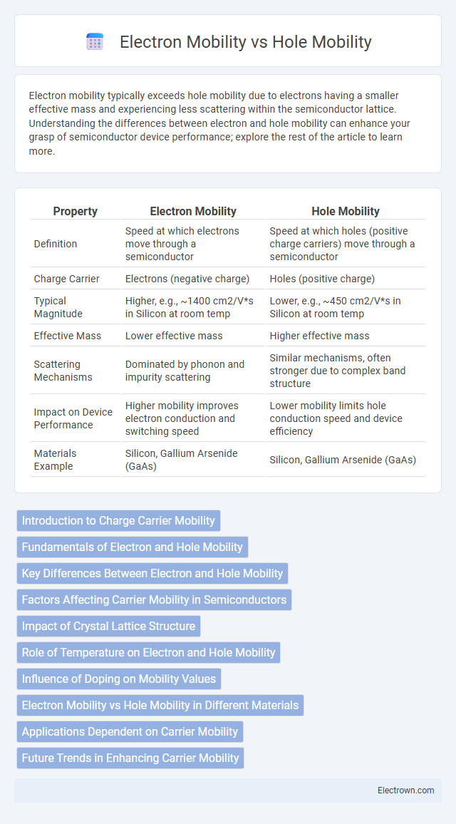
| Property | Electron Mobility | Hole Mobility |
|---|---|---|
| Definition | Speed at which electrons move through a semiconductor | Speed at which holes (positive charge carriers) move through a semiconductor |
| Charge Carrier | Electrons (negative charge) | Holes (positive charge) |
| Typical Magnitude | Higher, e.g., ~1400 cm2/V*s in Silicon at room temp | Lower, e.g., ~450 cm2/V*s in Silicon at room temp |
| Effective Mass | Lower effective mass | Higher effective mass |
| Scattering Mechanisms | Dominated by phonon and impurity scattering | Similar mechanisms, often stronger due to complex band structure |
| Impact on Device Performance | Higher mobility improves electron conduction and switching speed | Lower mobility limits hole conduction speed and device efficiency |
| Materials Example | Silicon, Gallium Arsenide (GaAs) | Silicon, Gallium Arsenide (GaAs) |
Introduction to Charge Carrier Mobility
Charge carrier mobility measures how quickly electrons or holes move through a semiconductor under an electric field. Electron mobility is typically higher than hole mobility due to differences in effective mass and scattering mechanisms within the crystal lattice. Understanding these mobility variations is essential for optimizing semiconductor device performance and material selection in electronics.
Fundamentals of Electron and Hole Mobility
Electron mobility refers to the ease with which electrons move through a semiconductor when subjected to an electric field, while hole mobility describes the corresponding movement of holes, or electron vacancies acting as positive charge carriers. Electron mobility is generally higher than hole mobility due to the smaller effective mass of electrons and less scattering compared to holes, which reside in the valence band with more complex band structures. Understanding the fundamental differences in effective mass, scattering mechanisms, and band structure is crucial for optimizing electronic device performance in semiconductors like silicon and gallium arsenide.
Key Differences Between Electron and Hole Mobility
Electron mobility typically exceeds hole mobility in most semiconductors due to electrons having smaller effective masses and experiencing less scattering. Holes, representing the absence of electrons in the valence band, exhibit lower mobility because they involve complex interactions with the crystal lattice and heavier effective masses. This disparity significantly affects the performance of devices like MOSFETs and bipolar transistors, where electron mobility enhances speed and conductivity more effectively than hole mobility.
Factors Affecting Carrier Mobility in Semiconductors
Electron mobility generally surpasses hole mobility due to the lower effective mass of electrons and their higher scattering rates in semiconductor materials. Carrier mobility in semiconductors is influenced by factors such as impurity concentration, lattice vibrations (phonon scattering), crystal defects, and temperature. The presence of impurities and defects increases ionized impurity scattering, while lattice vibrations intensify with temperature, both significantly reducing the mobility of electrons and holes.
Impact of Crystal Lattice Structure
Electron mobility typically exceeds hole mobility due to differences in effective mass and scattering mechanisms influenced by the crystal lattice structure. In materials with a highly symmetric lattice, electrons experience less scattering and higher mobility, whereas holes, which behave as positive charge carriers in the valence band, encounter more complex interactions with the lattice atoms. Your semiconductor device's performance can be optimized by selecting materials with lattice structures that favor higher electron mobility for faster switching speeds and better conductivity.
Role of Temperature on Electron and Hole Mobility
Temperature significantly influences electron and hole mobility in semiconductors by affecting lattice vibrations and scattering rates. As temperature rises, increased phonon scattering reduces both electron and hole mobility, with hole mobility typically decreasing more sharply due to heavier effective mass and stronger interaction with the lattice. Understanding the temperature dependence of electron and hole mobility is crucial for optimizing semiconductor device performance in varying thermal environments.
Influence of Doping on Mobility Values
Doping significantly affects electron and hole mobility by introducing impurities that alter the semiconductor's carrier concentration and scattering mechanisms. Electron mobility typically experiences less reduction than hole mobility when doped heavily because electrons, being lighter and more mobile, are less susceptible to impurity scattering. Understanding how your doping levels impact both electron and hole mobility is crucial for optimizing device performance, especially in silicon-based transistors.
Electron Mobility vs Hole Mobility in Different Materials
Electron mobility generally exceeds hole mobility in most semiconductor materials due to the smaller effective mass and higher velocity of electrons compared to holes. In silicon, electron mobility is approximately 1400 cm2/V*s, whereas hole mobility is around 450 cm2/V*s, highlighting the significant difference influenced by band structure and scattering mechanisms. Your choice of material heavily impacts device performance, as materials like gallium arsenide exhibit even higher electron mobilities, often exceeding 8000 cm2/V*s, while hole mobility remains comparatively lower.
Applications Dependent on Carrier Mobility
Electron mobility significantly exceeds hole mobility in most semiconductors, affecting the efficiency of electronic and optoelectronic devices. High electron mobility is crucial for applications like high-speed transistors and integrated circuits, where faster carrier transport enhances performance. Conversely, hole mobility becomes pivotal in p-type devices and organic semiconductors, influencing photovoltaic cells and flexible electronics where balanced carrier transport improves overall efficiency.
Future Trends in Enhancing Carrier Mobility
Future trends in enhancing carrier mobility emphasize advanced materials like two-dimensional semiconductors and novel heterostructures to improve electron mobility beyond conventional silicon limits. Techniques such as strain engineering and defect passivation target hole mobility enhancements critical for high-performance p-type transistors. Integration of these approaches aims to balance electron and hole mobilities, enabling faster, low-power CMOS devices in next-generation electronics.
Electron mobility vs Hole mobility Infographic