Anisotropic etching removes material at different rates depending on the crystal orientation, creating highly directional and precise patterns, while isotropic etching removes material uniformly in all directions, resulting in more rounded features. Understanding the distinctions between these etching techniques can help you select the best method for your microfabrication needs; continue reading to explore their applications and benefits.
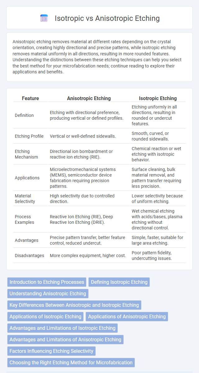
Table of Comparison
| Feature | Anisotropic Etching | Isotropic Etching |
|---|---|---|
| Definition | Etching with directional preference, producing vertical or defined profiles. | Etching uniformly in all directions, resulting in rounded or undercut features. |
| Etching Profile | Vertical or well-defined sidewalls. | Smooth, curved, or rounded sidewalls. |
| Etching Mechanism | Directional ion bombardment or reactive ion etching (RIE). | Chemical reaction or wet etching with isotropic behavior. |
| Applications | Microelectromechanical systems (MEMS), semiconductor device fabrication requiring precision patterns. | Surface cleaning, bulk material removal, and pattern transfer requiring less precision. |
| Material Selectivity | High selectivity due to controlled direction. | Lower selectivity because of uniform etching. |
| Process Examples | Reactive Ion Etching (RIE), Deep Reactive Ion Etching (DRIE). | Wet chemical etching with acids/bases, plasma etching without directional control. |
| Advantages | Precise pattern transfer, better feature control, reduced undercut. | Simple, faster, suitable for large area etching. |
| Disadvantages | More complex equipment, higher cost. | Poor pattern fidelity, undercutting issues. |
Introduction to Etching Processes
Etching processes play a critical role in microfabrication by selectively removing material to create intricate patterns on substrates. Anisotropic etching removes material at different rates depending on the crystal orientation, producing highly directional and precise features, while isotropic etching uniformly removes material in all directions, leading to rounded profiles. Your choice between anisotropic and isotropic etching depends on the desired pattern accuracy and feature shape in semiconductor manufacturing or MEMS device fabrication.
Defining Isotropic Etching
Isotropic etching removes material uniformly in all directions, resulting in rounded or undercut features due to equal lateral and vertical etch rates. This process is commonly used when precise pattern fidelity is less critical, but it can limit the resolution of microfabrication steps in semiconductor manufacturing. Understanding isotropic etching helps you choose the appropriate technique for applications requiring smooth, non-directional material removal.
Understanding Anisotropic Etching
Anisotropic etching selectively removes material in specific directions, resulting in highly controlled and precise microfabrication features crucial for semiconductor manufacturing. Unlike isotropic etching, which etches uniformly in all directions and creates rounded profiles, anisotropic etching produces sharp, well-defined edges by exploiting crystallographic orientation or directional plasma. Understanding anisotropic etching enables you to achieve accurate pattern transfer and enhanced device performance in MEMS and IC fabrication processes.
Key Differences Between Anisotropic and Isotropic Etching
Anisotropic etching removes material at different rates based on crystallographic orientation, resulting in well-defined, directional profiles ideal for precise microfabrication. Isotropic etching, by contrast, etches uniformly in all directions, producing rounded or undercut features suitable for applications where less geometric precision is required. Your choice between anisotropic and isotropic etching affects the accuracy, surface finish, and structural integrity of the final microelectronic or MEMS device.
Applications of Isotropic Etching
Isotropic etching is widely used in applications requiring uniform material removal regardless of direction, such as undercutting in microelectromechanical systems (MEMS) fabrication and patterning complex, curved surfaces. It is ideal for creating rounded or smooth feature edges in integrated circuit fabrication and for bulk silicon removal in sensor and microfluidic device manufacturing. The technique's ability to etch beneath masking layers makes it suitable for defining layers with precise thickness control in semiconductor processing.
Applications of Anisotropic Etching
Anisotropic etching is widely used in microfabrication processes where precise, directional material removal is critical, such as MEMS device manufacturing, microfluidic channel creation, and semiconductor wafer patterning. The controlled etching profile enables the formation of vertical sidewalls and high aspect ratio structures essential for device performance and integration. Your ability to achieve fine features and consistent geometries makes anisotropic etching indispensable in advanced electronics and microsystem applications.
Advantages and Limitations of Isotropic Etching
Isotropic etching provides uniform material removal in all directions, making it ideal for applications requiring smooth, rounded features and fast processing rates. Its main advantage lies in the simplicity and cost-effectiveness of chemical solutions used, which do not require complex equipment or directional control. However, isotropic etching lacks precision for fine pattern transfer and can undercut masks, limiting its suitability for high-resolution microfabrication tasks in advanced semiconductor devices.
Advantages and Limitations of Anisotropic Etching
Anisotropic etching offers superior precision by selectively removing material along specific crystallographic planes, enabling the creation of well-defined, high-aspect-ratio microstructures essential for MEMS and semiconductor devices. Its limitations include longer processing times and potential dependence on crystal orientation, which can restrict uniformity in complex geometries. Despite these challenges, anisotropic etching enhances device performance by providing better control over feature dimensions compared to isotropic etching methods.
Factors Influencing Etching Selectivity
Etching selectivity in anisotropic versus isotropic etching is influenced by factors such as the chemical composition of the etchant, substrate material properties, and etching conditions like temperature and pressure. Anisotropic etching typically depends on crystallographic orientation and reactive ion etching parameters to achieve directional material removal with high selectivity. In isotropic etching, uniform etchant diffusion and reaction rates dominate, resulting in less control over selectivity but consistent material dissolution.
Choosing the Right Etching Method for Microfabrication
Choosing the right etching method in microfabrication depends on the required precision and feature profile, with anisotropic etching providing directional material removal for high-aspect-ratio structures and isotropic etching offering uniform etching in all directions suitable for simpler geometries. Anisotropic etching techniques, such as reactive ion etching (RIE), enable the creation of vertical sidewalls essential for MEMS and semiconductor devices, while isotropic etching, like wet chemical etching, is often preferred for applications where undercutting is not critical. The decision balances etch profile control, selectivity, and process complexity to optimize device performance and manufacturing yield.
Anisotropic vs isotropic etching Infographic