The Czochralski method involves pulling a single crystal from a molten silicon bath, producing large-diameter wafers with controllable impurity levels, while the float zone technique purifies silicon by melting a small region and moving it along the ingot, resulting in extremely high-purity crystals with fewer defects. Understanding the differences between these growth methods can help you choose the optimal process for semiconductor applications--explore the full article to learn more.
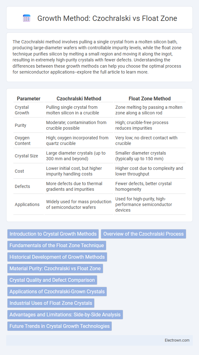
Table of Comparison
| Parameter | Czochralski Method | Float Zone Method |
|---|---|---|
| Crystal Growth | Pulling single crystal from molten silicon in a crucible | Zone melting by passing a molten zone along a silicon rod |
| Purity | Moderate; contamination from crucible possible | High; crucible-free process reduces impurities |
| Oxygen Content | High; oxygen incorporated from quartz crucible | Very low; no direct contact with crucible |
| Crystal Size | Large diameter crystals (up to 300 mm and beyond) | Smaller diameter crystals (typically up to 150 mm) |
| Cost | Lower initial cost, but higher impurity handling costs | Higher cost due to complexity and lower throughput |
| Defects | More defects due to thermal gradients and impurities | Fewer defects, better crystal homogeneity |
| Applications | Widely used for mass production of semiconductor wafers | Used for high-purity, high-performance semiconductor devices |
Introduction to Crystal Growth Methods
Czochralski and float zone are prominent crystal growth methods used to produce high-purity semiconductor wafers, essential for the electronics industry. The Czochralski method involves pulling a single crystal from a molten silicon bath, enabling large-diameter ingots with controlled doping, while the float zone technique uses localized heating to melt and recrystallize silicon, resulting in ultra-high purity crystals with minimal contamination. Both methods optimize crystal quality and defect minimization, but float zone offers superior purity due to its crucible-free process, making it ideal for high-performance applications.
Overview of the Czochralski Process
The Czochralski process involves melting high-purity semiconductor material in a crucible and slowly pulling a single crystal seed from the melt to form a large, cylindrical ingot. This method enables precise control over crystal diameter and doping levels, making it ideal for producing silicon wafers used in semiconductor devices. Your manufacturing efficiency benefits from the Czochralski process's ability to produce high-quality, uniform crystals at industrial scales.
Fundamentals of the Float Zone Technique
The Float Zone technique is a crystal growth method that involves melting a localized region of a semiconductor rod using an induction coil and moving this molten zone along the rod to purify and recrystallize the material. This process eliminates impurities by segregation and produces high-purity, high-resistivity silicon ideal for electronic applications. Your semiconductor manufacturing benefits from the Float Zone method's ability to create defect-free single crystals without contact with crucible materials, unlike the Czochralski method.
Historical Development of Growth Methods
The Czochralski method, developed by Jan Czochralski in 1916, revolutionized single crystal growth by enabling the controlled pulling of large, high-purity silicon crystals essential for early semiconductor technology. The float zone technique, introduced in the 1950s by Henry Theuerer at Bell Labs, advanced crystal purity further by refining silicon through zone melting without crucible contamination. Your choice between these growth methods depends on required crystal size, purity, and application in electronics manufacturing.
Material Purity: Czochralski vs Float Zone
The float zone method achieves higher material purity than the Czochralski process due to its crucible-free growth environment, which minimizes contamination and enables ultra-pure silicon crystals. In contrast, the Czochralski method involves a quartz crucible that can introduce oxygen impurities into the silicon material. For your semiconductor applications, selecting float zone silicon ensures superior purity essential for high-performance electronic devices.
Crystal Quality and Defect Comparison
The Czochralski method typically results in larger silicon wafers but may introduce oxygen-related defects due to the crucible's interaction, affecting crystal purity, whereas the float zone technique produces higher purity crystals with fewer oxygen and metallic impurities, enhancing overall crystal quality. Float zone crystals exhibit lower dislocation densities and reduced strain, making them ideal for high-performance semiconductor applications requiring superior electrical properties. Your choice between these growth methods should weigh the trade-off between wafer size and crystal defect concentration to optimize device performance.
Applications of Czochralski-Grown Crystals
Czochralski-grown crystals, characterized by their large diameter and high-quality single-crystal structure, are extensively utilized in semiconductor wafers for integrated circuits, solar cells, and LED manufacturing. This method supports control over dopant concentration, making it ideal for producing silicon and germanium crystals used in microelectronics and optoelectronics. The widespread application of Czochralski crystals in high-performance electronic devices highlights their essential role in advanced technology industries.
Industrial Uses of Float Zone Crystals
Float zone crystals are extensively used in industries requiring ultra-high purity silicon, such as semiconductor manufacturing and photovoltaic devices, because they minimize contamination and defects compared to Czochralski-grown crystals. Your advanced electronic components benefit from float zone silicon's superior electrical properties and high resistivity, which enhance device performance and reliability. This growth method is preferred in power electronics and high-frequency applications where material quality directly impacts efficiency.
Advantages and Limitations: Side-by-Side Analysis
The Czochralski method offers high throughput and scalable production, producing large-diameter silicon ingots ideal for semiconductor wafers, but it often introduces oxygen impurities that can affect device performance. The float zone technique produces ultra-pure crystals with minimal oxygen contamination, resulting in superior electronic properties, yet it is limited by smaller crystal size and higher production costs. Both methods balance trade-offs between purity, crystal size, and manufacturing efficiency, guiding their selection based on specific semiconductor quality and cost requirements.
Future Trends in Crystal Growth Technologies
Advancements in crystal growth technologies emphasize enhanced purity, controlled defect density, and scalability, with Czochralski (CZ) method evolving through innovations in thermal management and doping precision to support large-diameter silicon wafers for semiconductor industries. Float zone (FZ) technique trends focus on ultra-high purity and minimal oxygen contamination, crucial for high-performance power devices and specialty semiconductors, leveraging improved zone refining and in-situ monitoring. Integration of AI-driven process control and real-time diagnostics promises to optimize both CZ and FZ growth methods, accelerating development of next-generation electronic and photovoltaic materials.
Growth method: Czochralski vs float zone Infographic