Interdigitated layouts enable efficient electrode surface area utilization through alternating finger-like patterns, improving signal response and reducing parasitic capacitances compared to traditional pad layouts that rely on discrete contact points. Explore the rest of this article to understand which layout best suits your design needs and performance goals.
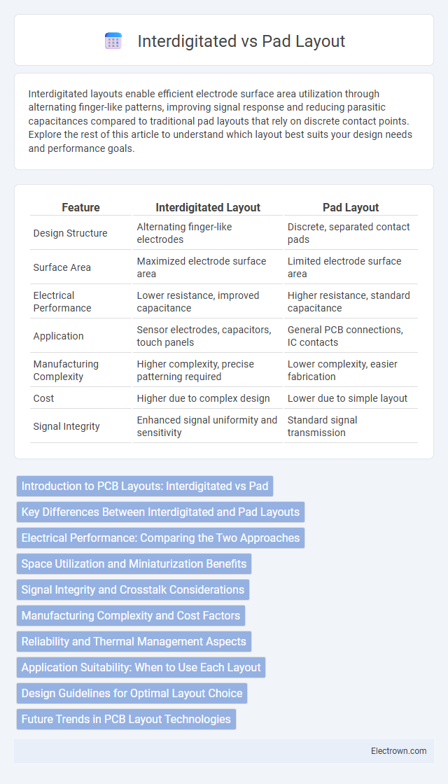
Table of Comparison
| Feature | Interdigitated Layout | Pad Layout |
|---|---|---|
| Design Structure | Alternating finger-like electrodes | Discrete, separated contact pads |
| Surface Area | Maximized electrode surface area | Limited electrode surface area |
| Electrical Performance | Lower resistance, improved capacitance | Higher resistance, standard capacitance |
| Application | Sensor electrodes, capacitors, touch panels | General PCB connections, IC contacts |
| Manufacturing Complexity | Higher complexity, precise patterning required | Lower complexity, easier fabrication |
| Cost | Higher due to complex design | Lower due to simple layout |
| Signal Integrity | Enhanced signal uniformity and sensitivity | Standard signal transmission |
Introduction to PCB Layouts: Interdigitated vs Pad
Interdigitated PCB layouts feature alternating finger-like conductive patterns, enhancing signal integrity and reducing crosstalk in high-frequency applications. Pad layouts consist of discrete, isolated contact points optimized for straightforward component placement and soldering processes. Selecting the appropriate layout affects your circuit's electrical performance, manufacturing complexity, and overall reliability.
Key Differences Between Interdigitated and Pad Layouts
Interdigitated layouts feature alternating fingers of electrodes that increase the active surface area and improve sensitivity in sensors, while pad layouts consist of separate, discrete electrode pads for simpler design and easier fabrication. Interdigitated designs are advantageous for applications requiring high-resolution capacitance measurements and enhanced signal-to-noise ratio, whereas pad layouts are often preferred for straightforward connectivity and electrical isolation. Your choice depends on the required performance characteristics, with interdigitated layouts benefiting high-precision sensors and pad layouts suiting basic circuit interfacing.
Electrical Performance: Comparing the Two Approaches
Interdigitated layouts minimize parasitic capacitance and resistance by interleaving electrode fingers, enhancing signal integrity and reducing noise in high-frequency applications. Pad layouts, featuring discrete, separated contact areas, often exhibit higher interconnect resistance and greater parasitic effects, which can impair electrical performance in densely packed circuits. The interdigitated approach generally offers superior current distribution and lower impedance, making it preferable for sensors, capacitors, and microelectronic devices requiring precise electrical characteristics.
Space Utilization and Miniaturization Benefits
Interdigitated layouts maximize space utilization by interlocking electrode fingers, creating a larger active surface area within a compact footprint, which significantly enhances miniaturization. Pad layouts, while simpler, tend to consume more space due to isolated electrode regions, limiting the potential for device size reduction. Choosing an interdigitated design optimizes your device's efficiency and enables advanced miniaturization in space-constrained applications.
Signal Integrity and Crosstalk Considerations
Interdigitated layouts reduce parasitic capacitance and inductance by distributing signal lines in an alternating pattern, significantly enhancing signal integrity in high-frequency circuits. In contrast, pad layouts tend to concentrate signals, increasing the risk of crosstalk and signal degradation due to closer line spacing and larger coupling areas. You can achieve superior noise immunity and minimized interference by choosing interdigitated designs, especially in sensitive mixed-signal or RF applications.
Manufacturing Complexity and Cost Factors
Interdigitated layouts involve alternating finger-like electrodes, increasing manufacturing complexity due to precise photolithography and alignment requirements, which can raise production costs compared to simpler pad layouts. Pad layouts feature larger, discrete electrode areas allowing easier fabrication with less stringent process controls, resulting in lower manufacturing costs. The choice between interdigitated and pad layouts impacts the overall device yield and material usage, influencing cost-efficiency in semiconductor and sensor manufacturing.
Reliability and Thermal Management Aspects
Interdigitated layouts offer enhanced reliability by providing improved current distribution and reducing localized heating compared to pad layouts, which tend to concentrate stress and hot spots. Effective thermal management in interdigitated designs ensures lower junction temperatures, extending device lifespan and performance stability under high-power conditions. Optimizing your circuit with interdigitated layouts can significantly reduce thermal resistance and enhance overall reliability in demanding applications.
Application Suitability: When to Use Each Layout
Interdigitated layouts excel in applications requiring high-density interconnections and improved signal integrity, making them ideal for sensors, capacitors, and electrodes in compact devices. Pad layouts are better suited for straightforward, easy-to-manufacture designs such as test points or simple interconnects where space efficiency and complexity are less critical. Choose your layout based on the complexity of the circuit, required performance, and manufacturing capabilities to ensure optimal functionality.
Design Guidelines for Optimal Layout Choice
Interdigitated layouts are ideal for maximizing surface area and improving charge collection efficiency in photovoltaic and sensor devices, while pad layouts simplify connectivity and reduce fabrication complexity. Your choice should consider factors like device size, electrical resistance, and manufacturing capabilities to ensure optimal performance and reliability. Adhering to design guidelines such as electrode spacing, finger width, and uniform current distribution will enhance the overall efficiency and functionality of your layout.
Future Trends in PCB Layout Technologies
Interdigitated and pad layouts in PCB design are evolving toward enhanced signal integrity and miniaturization to meet the demands of high-frequency applications and IoT devices. Emerging trends emphasize advanced materials with better thermal management, AI-driven design tools for optimal component placement, and 3D integration techniques that improve electrical performance and space efficiency. Your choice of layout will increasingly benefit from these innovations, enabling more reliable and compact electronic devices.
Interdigitated vs Pad layout Infographic