Latch-up occurs when a parasitic structure within a semiconductor device creates a low-resistance path, causing device failure due to excessive current flow, while snap-back refers to a sudden voltage drop in a device under stress, often used as a protective mechanism in ESD circuits. Understanding the differences between latch-up and snap-back is essential for improving your electronic circuit reliability; continue reading to explore their mechanisms and implications in detail.
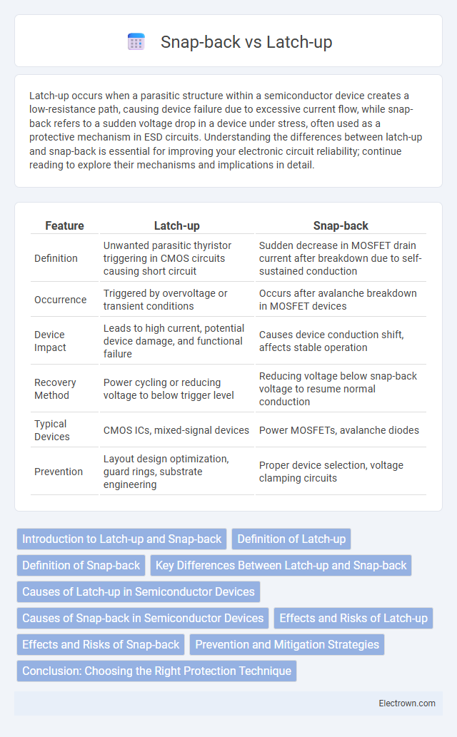
Table of Comparison
| Feature | Latch-up | Snap-back |
|---|---|---|
| Definition | Unwanted parasitic thyristor triggering in CMOS circuits causing short circuit | Sudden decrease in MOSFET drain current after breakdown due to self-sustained conduction |
| Occurrence | Triggered by overvoltage or transient conditions | Occurs after avalanche breakdown in MOSFET devices |
| Device Impact | Leads to high current, potential device damage, and functional failure | Causes device conduction shift, affects stable operation |
| Recovery Method | Power cycling or reducing voltage to below trigger level | Reducing voltage below snap-back voltage to resume normal conduction |
| Typical Devices | CMOS ICs, mixed-signal devices | Power MOSFETs, avalanche diodes |
| Prevention | Layout design optimization, guard rings, substrate engineering | Proper device selection, voltage clamping circuits |
Introduction to Latch-up and Snap-back
Latch-up is a parasitic structure that creates a short circuit in CMOS devices, causing high current flow and potential device failure. Snap-back refers to a sudden drop in voltage after a breakdown, often observed in bipolar transistors and MOSFETs during high voltage stress. Both phenomena are critical in semiconductor reliability and design, influencing protection circuits and device robustness.
Definition of Latch-up
Latch-up is a failure mechanism in CMOS devices caused by the inadvertent creation of a low-impedance path between the power supply rails, leading to high current flow and potential device damage. It occurs when parasitic thyristor structures within the integrated circuit are triggered by voltage or current transients. Preventing latch-up is critical for ensuring the reliability and stability of semiconductor circuits.
Definition of Snap-back
Snap-back refers to a semiconductor device behavior where, after an initial breakdown caused by excessive voltage, the device voltage rapidly decreases and stabilizes at a lower holding voltage while current continues to increase. This phenomenon occurs due to the activation of parasitic structures within the device, resulting in a sudden transition from high resistance to low resistance state. Understanding snap-back is crucial for preventing device failure in integrated circuits, particularly in bipolar junction transistors and power devices.
Key Differences Between Latch-up and Snap-back
Latch-up occurs in CMOS circuits when a parasitic thyristor forms, causing a low-impedance path and potentially leading to device failure, whereas snap-back is a voltage-controlled negative resistance effect observed in bipolar transistors during high current conditions. Latch-up typically results in permanent damage or requires a power cycle to clear, while snap-back is a transient phenomenon that can protect circuits by limiting voltage spikes. The key distinction lies in latch-up involving parasitic PNPN structures causing sustained conduction, whereas snap-back involves a temporary drop in voltage due to carrier injection in bipolar junctions.
Causes of Latch-up in Semiconductor Devices
Latch-up in semiconductor devices primarily occurs due to unintended parasitic thyristor structures formed within CMOS technology, caused by high current injection or voltage spikes that trigger a low-impedance path between power and ground. This effect often results from ionizing radiation, excessive transient voltage, or improper device layout, which allows the parasitic PNP and NPN transistors to create a regenerative feedback loop. To prevent latch-up, designers must optimize substrate doping, employ guard rings, and ensure adequate isolation between device regions.
Causes of Snap-back in Semiconductor Devices
Snap-back in semiconductor devices primarily occurs due to the impact ionization phenomenon within the device's parasitic bipolar transistor structure. This effect leads to a sudden drop in voltage as the device enters a low-resistance state, often triggered by high current densities or excessive injection levels. Understanding the causes of snap-back is crucial for designing robust integrated circuits that prevent latch-up and improve device reliability under stress conditions.
Effects and Risks of Latch-up
Latch-up in integrated circuits causes a low-impedance path between power and ground, potentially leading to excessive current flow and permanent damage to the device. This parasitic effect risks thermal runaway and device failure if not properly mitigated through design techniques. Protecting Your circuits from latch-up ensures enhanced reliability and prolonged operational life.
Effects and Risks of Snap-back
Snap-back causes a sudden return to a low voltage state after a high current trigger, potentially damaging semiconductor devices through localized heating and increased stress. This phenomenon can lead to permanent device failure or degraded performance by surpassing safe operating limits. Managing snap-back effects is crucial for your circuit reliability and long-term device stability.
Prevention and Mitigation Strategies
Latch-up prevention relies on layout techniques such as guard rings, substrate ties, and well contacts to minimize parasitic thyristor formation, alongside using low-resistance substrates and optimized doping profiles. Snap-back mitigation involves designing transistor geometries to reduce trigger sensitivity, implementing current-limiting resistors, and employing robust overvoltage protection circuits to prevent device instability. Both phenomena benefit from comprehensive simulation and layout verification to ensure reliable circuit operation under stress conditions.
Conclusion: Choosing the Right Protection Technique
Latch-up protection is essential for preventing permanent device damage caused by parasitic thyristor triggering, while snap-back protection effectively controls transient voltage by stabilizing device operation without destructive effects. Selecting the right technique depends on application requirements: latch-up protection suits CMOS circuits sensitive to high current spikes, whereas snap-back is ideal for safeguarding against voltage transients in protection devices like ESD clamps. Integrating both methods can enhance overall device reliability by addressing distinct failure mechanisms in semiconductor circuits.
Latch-up vs Snap-back Infographic