Vertical MOS transistors offer high current drive and better thermal performance, ideal for power applications, while lateral MOS transistors provide easier integration with standard CMOS processes and higher switching speeds. Explore the rest of the article to understand how these differences affect Your electronic circuit design choices.
Table of Comparison
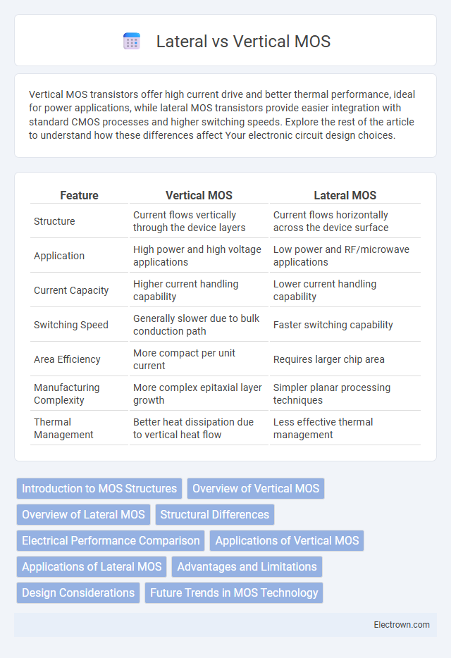
| Feature | Vertical MOS | Lateral MOS |
|---|---|---|
| Structure | Current flows vertically through the device layers | Current flows horizontally across the device surface |
| Application | High power and high voltage applications | Low power and RF/microwave applications |
| Current Capacity | Higher current handling capability | Lower current handling capability |
| Switching Speed | Generally slower due to bulk conduction path | Faster switching capability |
| Area Efficiency | More compact per unit current | Requires larger chip area |
| Manufacturing Complexity | More complex epitaxial layer growth | Simpler planar processing techniques |
| Thermal Management | Better heat dissipation due to vertical heat flow | Less effective thermal management |
Introduction to MOS Structures
Vertical MOS structures feature a current flow perpendicular to the substrate, optimizing space for high-power applications by stacking components vertically to enhance efficiency. Lateral MOS devices, in contrast, have current flow parallel to the surface, allowing for easier integration with other circuitry on a single chip and superior switching speeds. Understanding these fundamental differences helps you select the appropriate MOS structure for performance requirements such as power handling or switching frequency.
Overview of Vertical MOS
Vertical MOS transistors feature a structure where current flows vertically from source to drain, enabling higher current density and improved switching speeds. Commonly used in power electronics and high-frequency applications, vertical MOS devices offer enhanced thermal performance due to better heat dissipation through the substrate. Your choice of a vertical MOS transistor can significantly impact efficiency in high-power circuit designs.
Overview of Lateral MOS
Lateral Metal-Oxide-Semiconductor (MOS) transistors are designed with the current flowing parallel to the substrate surface, enabling easier integration in digital circuits with smaller footprints. These devices feature a lateral channel between the source and drain, which allows enhanced control of short-channel effects and reduces leakage currents. Lateral MOS transistors are widely used in CMOS technology for their compatibility with planar fabrication processes and efficient switching characteristics.
Structural Differences
Vertical MOSFETs feature a vertical current flow channel between the source and drain terminals, allowing for a compact design with a high-current capacity and efficient heat dissipation. Lateral MOSFETs have a horizontal current flow path on the chip surface, which simplifies manufacturing but limits current density and voltage handling capabilities. The structural difference in current flow orientation directly impacts device performance, scaling, and application suitability.
Electrical Performance Comparison
Vertical MOSFETs exhibit superior electrical performance in high-current and high-voltage applications due to their shorter current-carrying path and lower on-resistance, enabling more efficient power handling and reduced heat generation. Lateral MOSFETs offer advantages in low-voltage, signal-processing circuits with faster switching speeds and easier integration into compact IC layouts. Your choice between vertical and lateral MOS designs impacts device efficiency, switching performance, and thermal management, crucial for optimized circuit functionality.
Applications of Vertical MOS
Vertical MOSFETs are predominantly used in high-power and high-frequency applications such as power supplies, automotive electronics, and RF amplifiers due to their superior current handling and low on-resistance. Vertical MOS structures enable efficient heat dissipation and scalability, making them ideal for power management in electric vehicles and renewable energy systems. Their vertical conduction path allows for compact device layouts in power integrated circuits, enhancing overall system performance and reliability.
Applications of Lateral MOS
Lateral MOS transistors are widely used in analog circuits, RF switches, and power management applications due to their superior planar construction and ease of integration with standard CMOS processes. They provide high input impedance and fast switching speeds, making them ideal for signal amplification and low-noise applications. Lateral MOS devices are also preferred in monolithic microwave integrated circuits (MMICs) and RF front-end modules for wireless communication systems.
Advantages and Limitations
Vertical MOS transistors offer higher current density and better heat dissipation, making them ideal for high-power applications and integrated circuits in power management. Lateral MOS devices provide ease of fabrication and improved switching speeds, benefiting low-voltage digital circuits and RF applications. However, vertical MOS transistors face challenges in complex fabrication processes and higher cost, while lateral MOS devices exhibit limitations in handling high voltage and current due to their planar structure.
Design Considerations
Vertical MOS transistors are designed with current flow perpendicular to the wafer surface, enabling higher current density and better heat dissipation, making them ideal for power applications. Lateral MOS transistors feature current flow parallel to the wafer surface, allowing easier integration with other components in planar CMOS technology and offering better control of short-channel effects. Design considerations include application requirements, power handling, switching speed, and fabrication complexity, influencing the choice between vertical power MOSFETs and lateral MOSFETs in IC design.
Future Trends in MOS Technology
Future trends in MOS technology emphasize vertical MOSFETs due to their superior scalability and reduced on-resistance, enabling enhanced power efficiency in compact devices. Lateral MOS structures continue evolving with advanced materials like GaN and SiC to improve high-frequency performance and thermal management. Integration of vertical and lateral designs in hybrid architectures aims to optimize overall device functionality for next-generation power electronics and RF applications.
Vertical vs lateral MOS Infographic