Forward bias allows current to flow easily through a diode as the positive voltage is applied to the anode and negative to the cathode, reducing the barrier potential. Explore the rest of the article to understand how reverse bias prevents current flow and affects diode functionality in your electronic circuits.
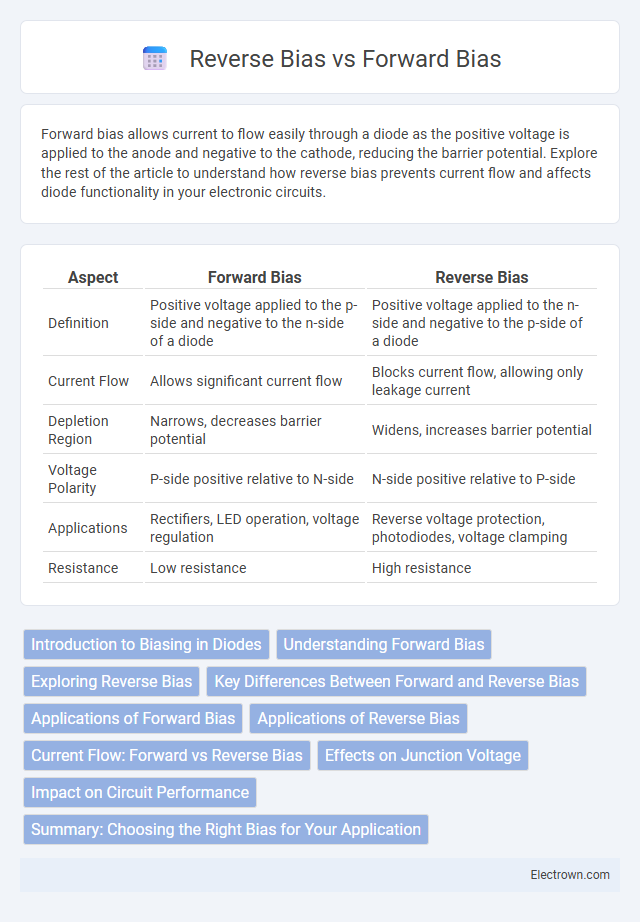
Table of Comparison
| Aspect | Forward Bias | Reverse Bias |
|---|---|---|
| Definition | Positive voltage applied to the p-side and negative to the n-side of a diode | Positive voltage applied to the n-side and negative to the p-side of a diode |
| Current Flow | Allows significant current flow | Blocks current flow, allowing only leakage current |
| Depletion Region | Narrows, decreases barrier potential | Widens, increases barrier potential |
| Voltage Polarity | P-side positive relative to N-side | N-side positive relative to P-side |
| Applications | Rectifiers, LED operation, voltage regulation | Reverse voltage protection, photodiodes, voltage clamping |
| Resistance | Low resistance | High resistance |
Introduction to Biasing in Diodes
Forward bias in diodes occurs when the positive terminal of a power source is connected to the anode and the negative to the cathode, allowing current to flow easily through the diode. Reverse bias happens when the polarity is reversed, creating a high resistance that prevents current flow, except for a minute leakage current. Understanding these biasing conditions helps you control the diode's operation in electronic circuits, enabling functions like rectification and signal modulation.
Understanding Forward Bias
Forward bias occurs when the positive terminal of a voltage source is connected to the p-type semiconductor and the negative terminal to the n-type, reducing the depletion region and allowing current to flow easily through a diode. This results in a low resistance path as the applied voltage overcomes the built-in potential barrier, enabling charge carriers to recombine across the junction. Forward bias is essential for diode operation in rectification, signaling, and switching applications, where controlled current conduction is required.
Exploring Reverse Bias
In reverse bias, a diode's positive terminal connects to the n-type material and the negative terminal to the p-type, causing the depletion region to widen and significantly reducing current flow to nearly zero, except for a minimal leakage current. This bias condition is essential for blocking current in circuits, enabling diodes to function as rectifiers and protectors against voltage spikes. Reverse bias voltage must not exceed the diode's breakdown voltage to prevent permanent damage or reverse breakdown effects.
Key Differences Between Forward and Reverse Bias
Forward bias occurs when the positive terminal of a power source connects to the p-type material and the negative terminal to the n-type, allowing current to flow easily through the diode. Reverse bias happens when the connections are reversed, with the positive terminal attached to the n-type and the negative to the p-type, preventing current flow and creating a depletion region. Your choice between forward and reverse bias directly impacts the diode's conductive state, influencing circuit behavior.
Applications of Forward Bias
Forward bias is essential in diode operation, allowing current to flow easily from the anode to the cathode, making it crucial in rectification processes such as AC to DC conversion in power supplies. It enables the functioning of light-emitting diodes (LEDs) by facilitating electron-hole recombination and photon emission. Forward bias is also fundamental in semiconductor devices like transistors, aiding signal amplification and switching applications in electronic circuits.
Applications of Reverse Bias
Reverse bias is primarily used in applications requiring high voltage blocking and minimal current flow, such as in diode rectifiers to prevent reverse current and protect circuits. It enables the functioning of photodiodes and solar cells by allowing the detection of light without significant current leakage. Furthermore, reverse bias conditions are critical in varactor diodes for voltage-controlled capacitance in tuning circuits and RF design.
Current Flow: Forward vs Reverse Bias
Current flow in forward bias occurs when the p-n junction allows charge carriers to move easily across the junction, resulting in a significant flow of current. In reverse bias, the depletion region widens, preventing charge carriers from crossing, leading to a negligible leakage current. Forward bias current typically ranges from microamperes to amperes, while reverse bias current remains in the nanoampere to microampere range.
Effects on Junction Voltage
In forward bias, the applied voltage reduces the potential barrier of the p-n junction, allowing current to flow easily as the junction voltage decreases typically to around 0.7 volts for silicon diodes. In reverse bias, the voltage increases the potential barrier, causing the junction voltage to rise and preventing current flow except for a minimal leakage current. This difference in junction voltage behavior under forward and reverse bias conditions is critical for the operation of diodes and other semiconductor devices.
Impact on Circuit Performance
Forward bias significantly enhances circuit performance by allowing current to flow through a diode, enabling efficient signal transmission and power regulation. Reverse bias restricts current flow, improving circuit protection by preventing leakage currents and minimizing noise, which preserves signal integrity. Understanding the impact of these biasing states helps you optimize device operation for desired electrical behavior.
Summary: Choosing the Right Bias for Your Application
Forward bias allows current to flow easily through a diode by reducing the barrier potential, making it ideal for circuits requiring conduction, such as rectifiers and LED operation. Reverse bias increases the barrier potential, preventing current flow and enabling applications like voltage regulation and signal isolation. Selecting the appropriate bias depends on whether you need current conduction or blocking in your electronic design.
Forward bias vs Reverse bias Infographic