Input capacitance affects how much charge is required to change a device's input voltage, influencing switching speed and signal integrity, while output capacitance governs how the output node stores and releases charge, impacting the output voltage stability and transient response. Understanding the differences between input and output capacitance is crucial for optimizing circuit performance and minimizing signal distortion, so explore the rest of the article to enhance Your knowledge in electronic design.
Table of Comparison
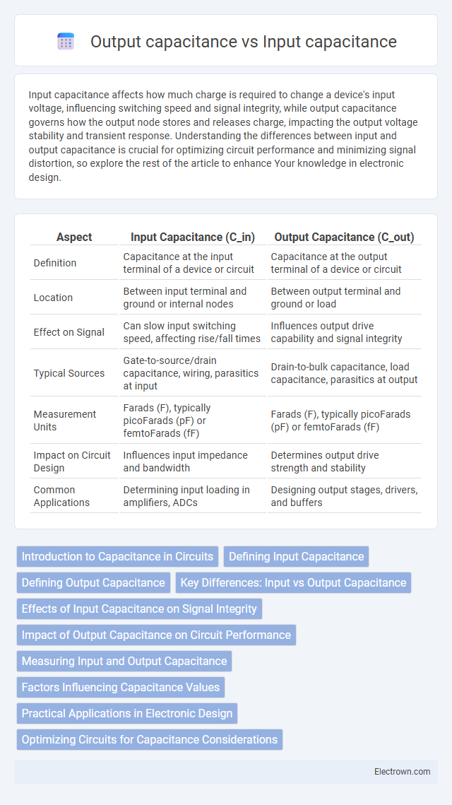
| Aspect | Input Capacitance (C_in) | Output Capacitance (C_out) |
|---|---|---|
| Definition | Capacitance at the input terminal of a device or circuit | Capacitance at the output terminal of a device or circuit |
| Location | Between input terminal and ground or internal nodes | Between output terminal and ground or load |
| Effect on Signal | Can slow input switching speed, affecting rise/fall times | Influences output drive capability and signal integrity |
| Typical Sources | Gate-to-source/drain capacitance, wiring, parasitics at input | Drain-to-bulk capacitance, load capacitance, parasitics at output |
| Measurement Units | Farads (F), typically picoFarads (pF) or femtoFarads (fF) | Farads (F), typically picoFarads (pF) or femtoFarads (fF) |
| Impact on Circuit Design | Influences input impedance and bandwidth | Determines output drive strength and stability |
| Common Applications | Determining input loading in amplifiers, ADCs | Designing output stages, drivers, and buffers |
Introduction to Capacitance in Circuits
Input capacitance refers to the effective capacitance presented at the input terminal of an electronic device or circuit, influencing signal integrity and bandwidth by affecting the load on the preceding stage. Output capacitance, on the other hand, is the capacitance seen at the output terminal, impacting the speed and stability of signal transmission to subsequent stages. Understanding these capacitances is crucial for optimizing high-frequency circuit performance and minimizing unwanted signal distortion or delay.
Defining Input Capacitance
Input capacitance refers to the capacitance present at the input terminal of an electronic component or device, representing the ability to store charge when a voltage is applied. It affects the signal rise time and bandwidth in circuits by influencing the input impedance and overall response speed. Understanding your device's input capacitance is crucial for optimizing high-frequency performance and ensuring accurate signal processing.
Defining Output Capacitance
Output capacitance refers to the intrinsic capacitance present at the output terminal of a semiconductor device, typically a transistor or MOSFET, which impacts switching speed and signal integrity. Unlike input capacitance that mainly affects the gate or control terminal, output capacitance influences the load-driving capability and overall power efficiency of the circuit. This parameter is critical in high-frequency applications where minimizing output capacitance reduces delay and power loss.
Key Differences: Input vs Output Capacitance
Input capacitance primarily affects the signal source by determining the load it experiences, influencing the speed and integrity of signal transmission into a device. Output capacitance impacts the device's ability to drive subsequent stages, affecting how quickly and efficiently it can charge or discharge connected loads. These differences are crucial in circuit design for optimizing performance, signal timing, and power consumption.
Effects of Input Capacitance on Signal Integrity
Input capacitance significantly influences signal integrity by causing signal distortion and slower rise times in high-frequency circuits. High input capacitance increases the RC time constant at the input node, leading to signal attenuation and potential timing errors in digital systems. Minimizing input capacitance is critical for maintaining fast signal transitions and reducing susceptibility to noise and signal reflection issues.
Impact of Output Capacitance on Circuit Performance
Output capacitance significantly affects circuit performance by influencing signal integrity, speed, and power consumption. Higher output capacitance slows down the output signal transition, leading to increased propagation delay and reduced switching speed in digital circuits. In analog applications, excessive output capacitance can cause stability issues and degrade frequency response, necessitating careful compensation and design considerations.
Measuring Input and Output Capacitance
Measuring input capacitance involves applying a small AC signal to the input terminal and observing the resulting current to determine the capacitive reactance, often using an LCR meter or impedance analyzer. Output capacitance measurement requires assessing the device's output node under no load or specific load conditions to capture the capacitive effects due to internal transistor junctions and packaging. Accurate measurement of both input and output capacitances is critical for optimizing high-frequency circuit performance and minimizing signal distortion in analog and digital systems.
Factors Influencing Capacitance Values
Input capacitance and output capacitance are influenced by device geometry, material properties, and operating conditions. Parameters such as transistor gate area, oxide thickness, and dielectric constant directly affect the input capacitance, while load impedance and parasitic effects primarily determine output capacitance. Understanding these factors helps optimize your circuit's performance by accurately predicting signal integrity and response times.
Practical Applications in Electronic Design
Input capacitance influences the speed and stability of signal reception in high-frequency circuits, crucial for optimizing your amplifier or ADC input stage performance. Output capacitance impacts the driving capability and signal integrity of output buffers and power transistors, directly affecting switching speeds and power efficiency in power electronics. Understanding these capacitances allows precise tuning of impedance matching and transient response in practical electronic design applications.
Optimizing Circuits for Capacitance Considerations
Input capacitance and output capacitance are critical parameters that influence the frequency response and stability of electronic circuits, with input capacitance affecting signal integrity at the source and output capacitance impacting load driving capability. Optimizing circuits for capacitance involves minimizing input capacitance to reduce signal distortion and selecting output capacitance values that balance speed and power consumption, particularly in high-frequency or high-speed applications. Careful layout design and component selection can mitigate parasitic capacitances, enhancing overall circuit performance and reliability.
Input capacitance vs Output capacitance Infographic