Intrinsic gain refers to the natural amplification provided by a device, such as a transistor, without any external components, while extrinsic gain involves the additional amplification achieved through external circuitry or feedback mechanisms. Understanding these differences can help you optimize your electronic designs for better performance; continue reading to explore practical applications and detailed comparisons.
Table of Comparison
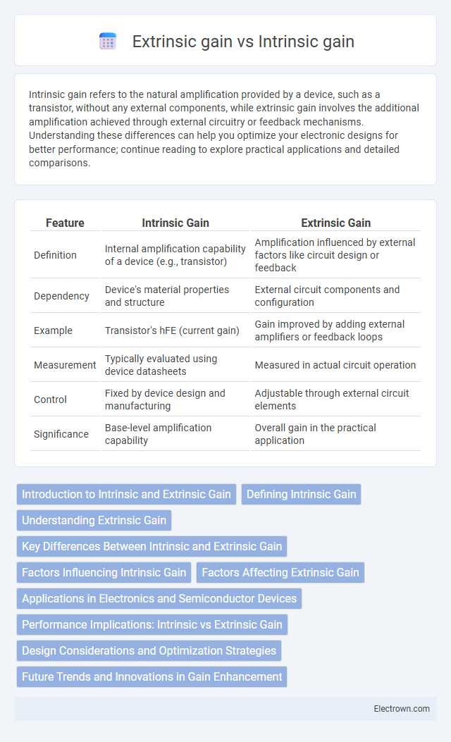
| Feature | Intrinsic Gain | Extrinsic Gain |
|---|---|---|
| Definition | Internal amplification capability of a device (e.g., transistor) | Amplification influenced by external factors like circuit design or feedback |
| Dependency | Device's material properties and structure | External circuit components and configuration |
| Example | Transistor's hFE (current gain) | Gain improved by adding external amplifiers or feedback loops |
| Measurement | Typically evaluated using device datasheets | Measured in actual circuit operation |
| Control | Fixed by device design and manufacturing | Adjustable through external circuit elements |
| Significance | Base-level amplification capability | Overall gain in the practical application |
Introduction to Intrinsic and Extrinsic Gain
Intrinsic gain refers to the amplification capability inherent within a transistor, determined by its internal physical properties and design structure. Extrinsic gain, on the other hand, encompasses the overall gain of a transistor including both intrinsic gain and the effects of external circuit elements such as resistors and capacitors. Understanding the distinction between intrinsic and extrinsic gain is crucial for optimizing transistor performance in analog circuit design.
Defining Intrinsic Gain
Intrinsic gain refers to the inherent amplification capability of a transistor or amplifier device, primarily determined by its internal physical properties such as transconductance and output resistance. It represents the maximum voltage gain achievable without external components or feedback circuits. Understanding intrinsic gain is crucial for designing high-performance analog circuits where amplification efficiency and signal integrity are essential.
Understanding Extrinsic Gain
Extrinsic gain refers to the amplification factor of a transistor calculated using the actual circuit configuration, including the effects of external components and load conditions. It differs from intrinsic gain, which measures the transistor's inherent amplification capability without external influence. Understanding extrinsic gain is crucial for accurate performance prediction in real-world applications and optimizing circuit design for stability and efficiency.
Key Differences Between Intrinsic and Extrinsic Gain
Intrinsic gain refers to the amplification capability inherent within a transistor or semiconductor device, fundamentally determined by its physical properties such as carrier mobility and device geometry. Extrinsic gain incorporates external circuit elements like resistors and capacitors that influence overall gain, often resulting in increased output but potentially reduced bandwidth or stability. Key differences include intrinsic gain's reliance on device-level parameters versus extrinsic gain's dependence on circuit-level design, impacting performance metrics such as frequency response and signal integrity.
Factors Influencing Intrinsic Gain
Intrinsic gain in transistors primarily depends on device physics factors such as carrier mobility, channel length, and oxide thickness, which influence the transistor's ability to amplify signals internally. Variations in semiconductor material quality, temperature, and doping concentrations also significantly affect intrinsic gain by altering charge carrier behavior. You can optimize intrinsic gain through careful engineering of these parameters, distinct from extrinsic gain factors like external circuit elements and parasitic resistances.
Factors Affecting Extrinsic Gain
Extrinsic gain in transistors is primarily influenced by external circuit elements such as load resistance, feedback networks, and the biasing configuration, which modify the overall voltage amplification beyond the device's intrinsic capabilities. Parasitic capacitances and resistances in the device packaging and interconnections also impact extrinsic gain by introducing frequency-dependent attenuation and phase shifts. Temperature variations and manufacturing differences can alter these external factors, causing fluctuations in the extrinsic gain performance across different operating conditions.
Applications in Electronics and Semiconductor Devices
Intrinsic gain, derived from the fundamental properties of semiconductor materials such as carrier mobility and channel length, is crucial for designing high-performance transistors in integrated circuits and analog amplifiers. Extrinsic gain incorporates external circuit elements and parasitic effects, influencing overall device efficiency in applications like radio frequency (RF) amplifiers, sensors, and communication systems. Optimizing both intrinsic and extrinsic gain enables semiconductor devices to achieve enhanced signal amplification, improved noise margins, and greater linearity in electronic applications.
Performance Implications: Intrinsic vs Extrinsic Gain
Intrinsic gain directly impacts transistor performance by influencing the device's transconductance and cut-off frequency, leading to faster switching speeds and improved amplification efficiency. Extrinsic gain, affected by external circuit elements such as load resistance and parasitic capacitances, often reduces the overall gain and bandwidth due to additional signal losses and noise. Optimizing intrinsic gain through material quality and device architecture is critical for high-performance analog and RF circuits, whereas controlling extrinsic gain necessitates careful circuit design and layout to minimize detrimental effects.
Design Considerations and Optimization Strategies
Intrinsic gain depends on the transistor's physical properties such as transconductance (gm) and output conductance (gds), requiring careful material selection and device scaling to enhance performance. Extrinsic gain involves external circuit elements like load resistance and feedback networks, making layout optimization and parasitic reduction critical to maximize the overall amplifier gain. You can achieve optimal amplifier design by balancing intrinsic device characteristics with precise external component tuning and minimizing signal loss throughout the signal path.
Future Trends and Innovations in Gain Enhancement
Intrinsic gain improvements leverage advanced semiconductor materials like GaN and SiC, enabling devices to achieve higher electron mobility and thermal stability, which boost performance in high-frequency and high-power applications. Extrinsic gain enhancements focus on innovative circuit design techniques such as feedback control, adaptive biasing, and novel transistor architectures to optimize overall amplification efficiency. Your choice of gain strategy must consider emerging trends like AI-driven design automation and nanotechnology integration, which promise to revolutionize gain enhancement in next-generation electronic devices.
Intrinsic gain vs Extrinsic gain Infographic